Datasheet AEM00940 (E-peas) - 3
| Производитель | E-peas |
| Описание | Highly efficient, regulated dual-output, ambient energy manager for Source Voltage Level Configuration with optional primary battery |
| Страниц / Страница | 29 / 3 — DATASHEET. AEM00940. List of Figures |
| Формат / Размер файла | PDF / 2.2 Мб |
| Язык документа | английский |
DATASHEET. AEM00940. List of Figures

Модельный ряд для этого даташита
Текстовая версия документа
link to page 5 link to page 6 link to page 10 link to page 11 link to page 11 link to page 14 link to page 17 link to page 18 link to page 19 link to page 19 link to page 20 link to page 21 link to page 22 link to page 22 link to page 23 link to page 23 link to page 24 link to page 25 link to page 26 link to page 28 link to page 28 link to page 28
DATASHEET AEM00940 List of Figures
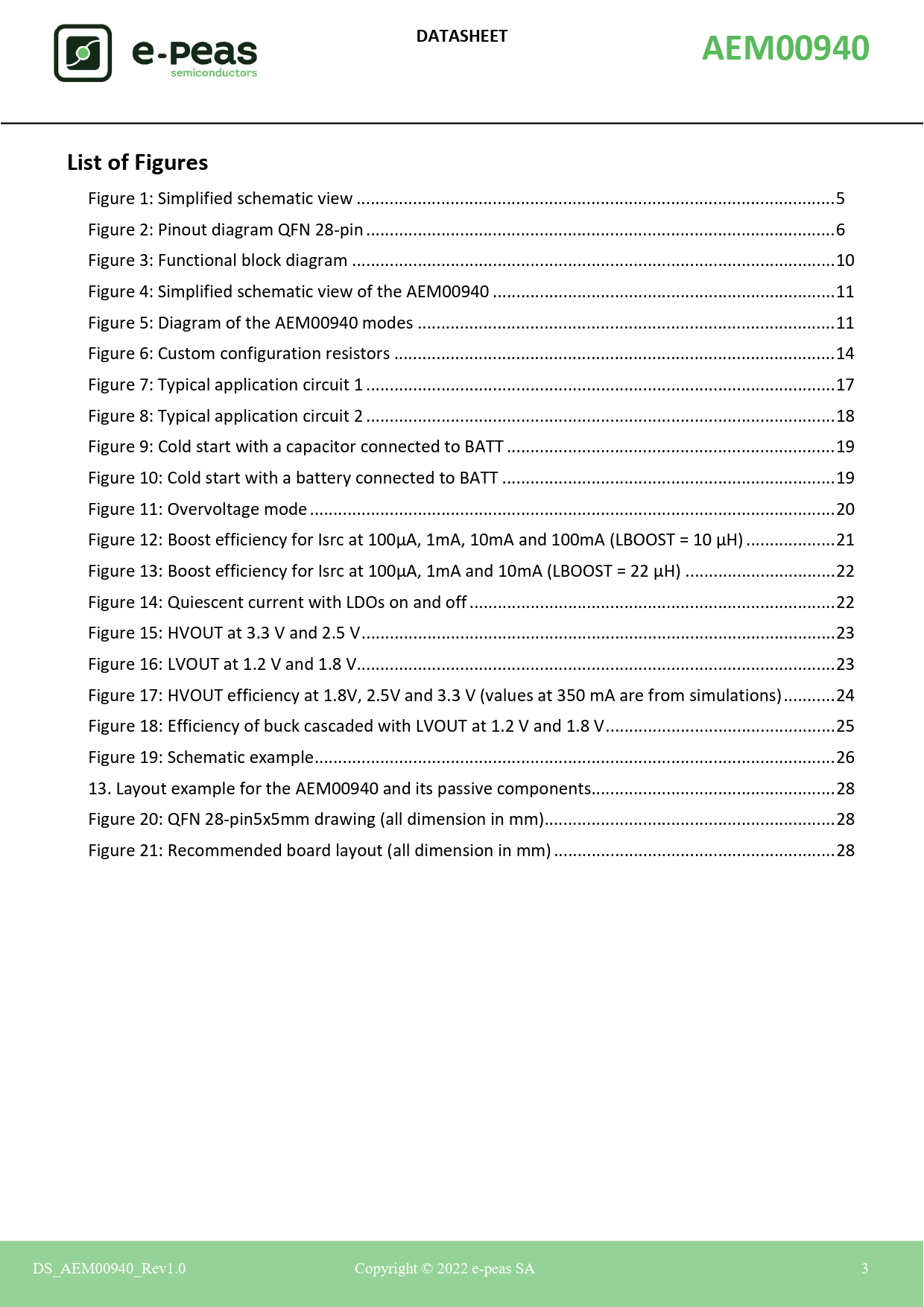
Figure 1: Simplified schematic view . 5 Figure 2: Pinout diagram QFN 28-pin. 6 Figure 3: Functional block diagram . .10 Figure 4: Simplified schematic view of the AEM00940 . .11 Figure 5: Diagram of the AEM00940 modes . .11 Figure 6: Custom configuration resistors . 14 Figure 7: Typical application circuit 1 . 17 Figure 8: Typical application circuit 2 . 18 Figure 9: Cold start with a capacitor connected to BATT . 19 Figure 10: Cold start with a battery connected to BATT . .19 Figure 11: Overvoltage mode. 20 Figure 12: Boost efficiency for Isrc at 100µA, 1mA, 10mA and 100mA (LBOOST = 10 µH) . .21 Figure 13: Boost efficiency for Isrc at 100µA, 1mA and 10mA (LBOOST = 22 µH) . 22 Figure 14: Quiescent current with LDOs on and off. 22 Figure 15: HVOUT at 3.3 V and 2.5 V. .23 Figure 16: LVOUT at 1.2 V and 1.8 V. 23 Figure 17: HVOUT efficiency at 1.8V, 2.5V and 3.3 V (values at 350 mA are from simulations). .24 Figure 18: Efficiency of buck cascaded with LVOUT at 1.2 V and 1.8 V. .25 Figure 19: Schematic example. .26 13. Layout example for the AEM00940 and its passive components. 28 Figure 20: QFN 28-pin5x5mm drawing (al dimension in mm). 28 Figure 21: Recommended board layout (al dimension in mm). 28 DS_AEM00940_Rev1.0 Copyright © 2022 e-peas SA 3 Document Outline 1. Introduction 2. Absolute Maximum Ratings 3. Thermal Resistance 4. Typical Electrical Characteristics at 25 °C 5. Recommended Operation Conditions 6. Functional Block Diagram 7. Theory of Operation 7.1. Deep sleep & Wake up modes 7.1.1. Supercapacitor as a storage element. 7.1.2. Battery as a storage element. 7.2. Normal mode 7.2.1. Boost 7.2.2. Buck 7.2.3. LDO outputs 7.3. Overcharge mode 7.4. Primary mode 7.5. Shutdown mode 7.6. Balun for dual-cell supercapacitor 8. System configuration 8.1. Battery and LDOs configuration 8.1.1. Custom mode 8.2. Source voltage configuration 8.3. Primary battery configuration 8.4. No-battery configuration 8.5. Storage element information 8.6. External inductors information 8.7. External capacitors information 9. Typical Application Circuits 9.1. Example circuit 1 9.2. Example circuit 2 10. Performance Data 10.1. BOOST conversion efficiency for LBOOST = 10 µH 10.2. BOOST conversion efficiency for LBOOST = 22 µH 10.3. Quiescent current 10.4. High-voltage LDO regulation 10.5. Low-voltage LDO regulation 10.6. High-voltage LDO efficiency 10.7. Low-voltage LDO efficiency 11. Schematic 12. Layout Package Information 13.1. Plastic Quad Flatpack No-lead (QFN 28-pin 5x5mm) 13.2. Board Layout 14. Revision History