Datasheet ADCMP609 (Analog Devices)
| Производитель | Analog Devices |
| Описание | Rail-to-Rail, Fast, Low Power 2.5 V to 5.5 V, Single-Supply TTL/CMOS Comparator |
| Страниц / Страница | 12 / 1 — Rail-to-Rail, Fast, Low Power 2.5 V to 5.5 V,. Single-Supply TTL/CMOS … |
| Версия | C |
| Формат / Размер файла | PDF / 265 Кб |
| Язык документа | английский |
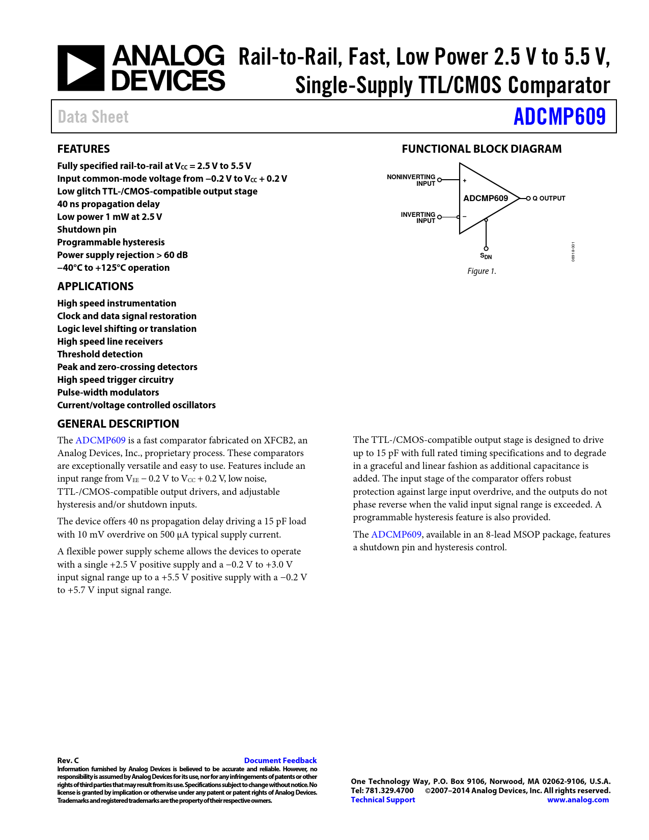
Rail-to-Rail, Fast, Low Power 2.5 V to 5.5 V,. Single-Supply TTL/CMOS Comparator. Data Sheet. ADCMP609. FEATURES

59 предложений от 28 поставщиков Микросхема Компаратор, ANALOG DEVICES ADCMP609BRMZ Analog Comparator, Single, High Speed, 1, 40ns, 2.5V to 5.5V, MSOP, 8Pins |
| ADCMP609BRMZ
Analog Devices | 114 ₽ | |
| ADCMP609BRMZ-REEL
Analog Devices | 119 ₽ | |
| ADCMP609BRMZ-REEL7
Analog Devices | 365 ₽ | |
| ADCMP609BRMZ-REEL7
Analog Devices | по запросу | |
Модельный ряд для этого даташита
Текстовая версия документа
Rail-to-Rail, Fast, Low Power 2.5 V to 5.5 V, Single-Supply TTL/CMOS Comparator Data Sheet ADCMP609 FEATURES FUNCTIONAL BLOCK DIAGRAM Fully specified rail-to-rail at VCC = 2.5 V to 5.5 V Input common-mode voltage from −0.2 V to VCC + 0.2 V NONINVERTING + INPUT Low glitch TTL-/CMOS-compatible output stage 40 ns propagation delay ADCMP609 Q OUTPUT Low power 1 mW at 2.5 V INVERTING – INPUT Shutdown pin Programmable hysteresis
001
Power supply rejection > 60 dB SDN
06918-
−40°C to +125°C operation
Figure 1.
APPLICATIONS High speed instrumentation Clock and data signal restoration Logic level shifting or translation High speed line receivers Threshold detection Peak and zero-crossing detectors High speed trigger circuitry Pulse-width modulators Current/voltage controlled oscillators GENERAL DESCRIPTION
The ADCMP609 is a fast comparator fabricated on XFCB2, an The TTL-/CMOS-compatible output stage is designed to drive Analog Devices, Inc., proprietary process. These comparators up to 15 pF with full rated timing specifications and to degrade are exceptionally versatile and easy to use. Features include an in a graceful and linear fashion as additional capacitance is input range from VEE − 0.2 V to VCC + 0.2 V, low noise, added. The input stage of the comparator offers robust TTL-/CMOS-compatible output drivers, and adjustable protection against large input overdrive, and the outputs do not hysteresis and/or shutdown inputs. phase reverse when the valid input signal range is exceeded. A The device offers 40 ns propagation delay driving a 15 pF load programmable hysteresis feature is also provided. with 10 mV overdrive on 500 µA typical supply current. The ADCMP609, available in an 8-lead MSOP package, features A flexible power supply scheme allows the devices to operate a shutdown pin and hysteresis control. with a single +2.5 V positive supply and a −0.2 V to +3.0 V input signal range up to a +5.5 V positive supply with a −0.2 V to +5.7 V input signal range.
Rev. C Document Feedback Information furnished by Analog Devices is believed to be accurate and reliable. However, no responsibility is assumed by Analog Devices for its use, nor for any infringements of patents or other rights of third parties that may result from its use. Specifications subject to change without notice. No One Technology Way, P.O. Box 9106, Norwood, MA 02062-9106, U.S.A. license is granted by implication or otherwise under any patent or patent rights of Analog Devices. Tel: 781.329.4700 ©2007–2014 Analog Devices, Inc. All rights reserved. Trademarks and registered trademarks are the property of their respective owners. Technical Support www.analog.com
Document Outline FEATURES APPLICATIONS FUNCTIONAL BLOCK DIAGRAM GENERAL DESCRIPTION TABLE OF CONTENTS REVISION HISTORY SPECIFICATIONS ELECTRICAL CHARACTERISTICS ABSOLUTE MAXIMUM RATINGS THERMAL RESISTANCE ESD CAUTION PIN CONFIGURATION AND FUNCTION DESCRIPTIONS TYPICAL PERFORMANCE CHARACTERISTICS APPLICATIONS INFORMATION POWER/GROUND LAYOUT AND BYPASSING TTL-/CMOS-COMPATIBLE OUTPUT STAGE OPTIMIZING PERFORMANCE COMPARATOR PROPAGATION DELAY DISPERSION COMPARATOR HYSTERESIS CROSSOVER BIAS POINT MINIMUM INPUT SLEW RATE REQUIREMENT TYPICAL APPLICATIONS CIRCUITS OUTLINE DIMENSIONS ORDERING GUIDE
 Купить ADCMP609BRMZ на РадиоЛоцман.Цены — от 40 до 365 ₽