Datasheet ADN2891 (Analog Devices)
| Производитель | Analog Devices |
| Описание | 3.3 V, 3.2 Gbps Limiting Amplifier |
| Страниц / Страница | 16 / 1 — 3.3 V, 3.2 Gbps,. Limiting Amplifier. Data Sheet. ADN2891. FEATURES. … |
| Версия | B |
| Формат / Размер файла | PDF / 603 Кб |
| Язык документа | английский |
3.3 V, 3.2 Gbps,. Limiting Amplifier. Data Sheet. ADN2891. FEATURES. GENERAL DESCRIPTION. Input sensitivity: 4 mV p-p

15 предложений от 13 поставщиков Микросхема Буферный усилитель, ANALOG DEVICES ADN2891ACPZ-RL7 Limiting Amplifier, 2.9V, 3.6V, LFCSP, 16Pins, -40℃ |
| ADN2891ACPZ-RL7
Analog Devices | 265 ₽ | |
| ADN2891ACPZ-RL7
Analog Devices | 327 ₽ | |
| ADN2891ACPZ-RL7
Analog Devices | от 1 393 ₽ | |
| ADN2891ACPZ-RL7
Analog Devices | по запросу | |
Модельный ряд для этого даташита
Текстовая версия документа
3.3 V, 3.2 Gbps, Limiting Amplifier Data Sheet ADN2891 FEATURES GENERAL DESCRIPTION Input sensitivity: 4 mV p-p
The ADN2891 is a 3.2 Gbps limiting amplifier with integrated
80 ps rise/fall times
loss-of-signal (LOS) detection circuitry and a received signal
CML outputs: 700 mV p-p differential
strength indicator (RSSI). This part is optimized for SONET,
Programmable LOS detector: 3.5 mV to 35 mV
Gigabit Ethernet (GbE), and Fibre Channel optoelectronic
Rx signal strength indicator (RSSI)
conversion applications. The ADN2891 has a differential input
SFF-8472-compliant average power measurement
sensitivity of 4 mV p-p and accepts up to a 2.0 V p-p differential
Single-supply operation: 3.3 V
input overload voltage. The ADN2891 supports current mode
Low power dissipation: 145 mW
logic (CML) outputs with controlled rise and fall times.
Available in space-saving 3 mm × 3 mm, 16-lead LFCSP
By monitoring the bias current through a photodiode, the on-
Extended temperature range: −40°C to +95°C
chip RSSI detector measures the average power received with
SFP reference design available
2% typical linearity over the entire valid input range of the photodiode. The on-chip RSSI detector facilitates SFF-8472-
APPLICATIONS
compliant optical transceivers by eliminating the need for
SFP/SFF/GBIC optical transceivers
external RSSI detector circuitry.
OC-3/OC-12/OC-48, GbE, Fibre Channel (FC) receivers
Additional features include a programmable loss-of-signal
10GBASE-LX4 transceivers
(LOS) detector and output squelch.
WDM transponders
The ADN2891 is available in a 3 mm × 3 mm, 16-lead LFCSP.
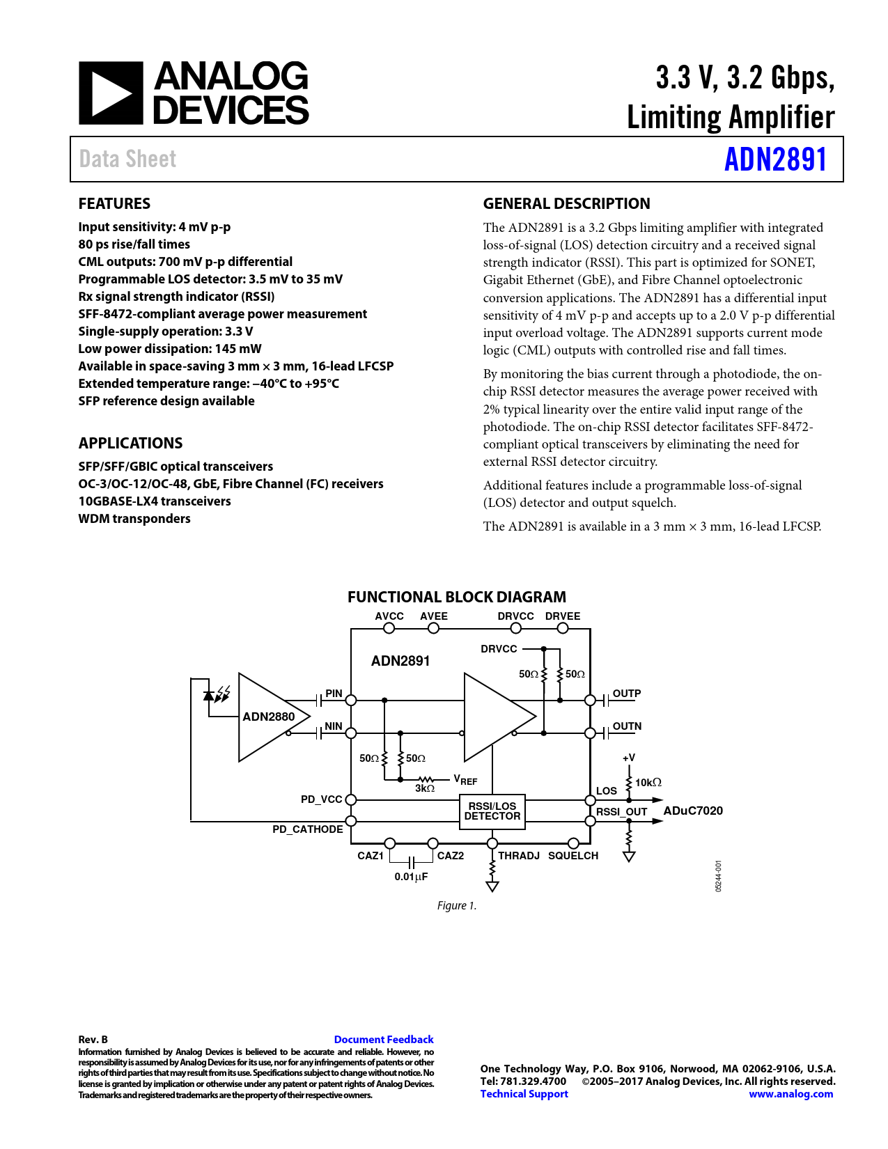
FUNCTIONAL BLOCK DIAGRAM AVCC AVEE DRVCC DRVEE DRVCC ADN2891 50
Ω
50
Ω
PIN OUTP ADN2880 NIN OUTN 50
Ω
50
Ω
+V VREF 10k
Ω
3k
Ω
LOS PD_VCC RSSI/LOS RSSI_OUT ADuC7020 DETECTOR PD_CATHODE CAZ1 CAZ2 THRADJ SQUELCH 0.01
µ
F
05244-001 Figure 1.
Rev. B Document Feedback Information furnished by Analog Devices is believed to be accurate and reliable. However, no responsibility is assumed by Analog Devices for its use, nor for any infringements of patents or other rights of third parties that may result from its use. Specifications subject to change without notice. No One Technology Way, P.O. Box 9106, Norwood, MA 02062-9106, U.S.A. license is granted by implication or otherwise under any patent or patent rights of Analog Devices. Tel: 781.329.4700 ©2005–2017 Analog Devices, Inc. All rights reserved. Trademarks and registered trademarks are the property of their respective owners. Technical Support www.analog.com
Document Outline FEATURES APPLICATIONS GENERAL DESCRIPTION FUNCTIONAL BLOCK DIAGRAM SPECIFICATIONS ABSOLUTE MAXIMUM RATINGS THERMAL RESISTANCE ESD CAUTION PIN CONFIGURATION AND FUNCTION DESCRIPTIONS TYPICAL PERFORMANCE CHARACTERISTICS THEORY OF OPERATION LIMITING AMPLIFIER Input Buffer CML Output Buffer LOSS OF SIGNAL (LOS) DETECTOR RECEIVED SIGNAL STRENGTH INDICATOR (RSSI) SQUELCH MODE APPLICATIONS PCB DESIGN GUIDELINES Output Buffer Power Supply and Ground Planes PCB Layout Soldering Guidelines for the LFCSP OUTLINE DIMENSIONS ORDERING GUIDE
 Купить ADN2891ACPZ-RL7 на РадиоЛоцман.Цены — от 44 до 1 393 ₽