Datasheet ADRF6520 (Analog Devices)
| Производитель | Analog Devices |
| Описание | Dual Programmable Filters and VGAs for 2 GHz Channel Spacing for μW Radios |
| Страниц / Страница | 29 / 1 — Dual Programmable Filters and VGAs for. 2 GHz Channel Spacing for µW … |
| Формат / Размер файла | PDF / 1.6 Мб |
| Язык документа | английский |
Dual Programmable Filters and VGAs for. 2 GHz Channel Spacing for µW Radios. Data Sheet. ADRF6520. FEATURES

Модельный ряд для этого даташита
Текстовая версия документа
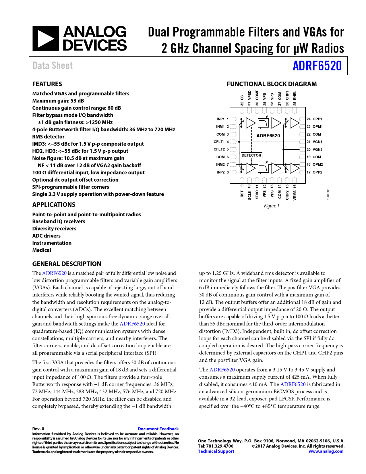
Dual Programmable Filters and VGAs for 2 GHz Channel Spacing for µW Radios Data Sheet ADRF6520 FEATURES FUNCTIONAL BLOCK DIAGRAM Matched VGAs and programmable filters D 1 M M NBL Maximum gain: 53 dB CS VPSD CO VPS VPS CO CHP E 32 31 30 29 28 27 26 25 Continuous gain control range: 60 dB Filter bypass mode I/Q bandwidth ±1 dB gain flatness: >1250 MHz INP1 1 24 OPP1 4-pole Butterworth filter I/Q bandwidth: 36 MHz to 720 MHz INM1 2 23 OPM1 RMS detector COM 3 22 COM ADRF6520 IMD3: <−55 dBc for 1.5 V p-p composite output CFLT1 4 21 VGN1 HD2, HD3: <−55 dBc for 1.5 V p-p output CFLT2 5 20 VGN2 Noise figure: 10.5 dB at maximum gain DETECTOR COM 6 19 COM NF < 11 dB over 12 dB of VGA2 gain backoff INM2 7 18 OPM2 100 Ω differential input, low impedance output INP2 8 17 OPP2 Optional dc output offset correction SPI-programmable filter corners 9 10 11 12 13 14 15 16 Single 3.3 V supply operation with power-down feature T K O M 2
001
MS RS CL DI VPS VPS S S CO CHP VR
14830-
APPLICATIONS
Figure 1
Point-to-point and point-to-multipoint radios Baseband IQ receivers Diversity receivers ADC drivers Instrumentation Medical GENERAL DESCRIPTION
The ADRF6520 is a matched pair of ful y differential low noise and up to 1.25 GHz. A wideband rms detector is available to low distortion programmable filters and variable gain amplifiers monitor the signal at the filter inputs. A fixed gain amplifier of (VGAs). Each channel is capable of rejecting large, out of band 6 dB immediately fol ows the filter. The postfilter VGA provides interferers while reliably boosting the wanted signal, thus reducing 30 dB of continuous gain control with a maximum gain of the bandwidth and resolution requirements on the analog-to- 12 dB. The output buffers offer an additional 18 dB of gain and digital converters (ADCs). The excellent matching between provide a differential output impedance of 20 Ω. The output channels and their high spurious-free dynamic range over al buffers are capable of driving 1.5 V p-p into 100 Ω loads at better gain and bandwidth settings make the ADRF6520 ideal for than 55 dBc nominal for the third-order intermodulation quadrature-based (IQ) communication systems with dense distortion (IMD3). Independent, built in, dc offset correction constellations, multiple carriers, and nearby interferers. The loops for each channel can be disabled via the SPI if fully dc- filter corners, enable, and dc offset correction loop enable are coupled operation is desired. The high-pass corner frequency is all programmable via a serial peripheral interface (SPI). determined by external capacitors on the CHP1 and CHP2 pins The first VGA that precedes the filters offers 30 dB of continuous and the postfilter VGA gain. gain control with a maximum gain of 18 dB and sets a differential The ADRF6520 operates from a 3.15 V to 3.45 V supply and input impedance of 100 Ω. The filters provide a four-pole consumes a maximum supply current of 425 mA. When ful y Butterworth response with −1 dB corner frequencies: 36 MHz, disabled, it consumes ≤10 mA. The ADRF6520 is fabricated in 72 MHz, 144 MHz, 288 MHz, 432 MHz, 576 MHz, and 720 MHz. an advanced silicon-germanium BiCMOS process and is For operation beyond 720 MHz, the filter can be disabled and available in a 32-lead, exposed pad LFCSP. Performance is completely bypassed, thereby extending the −1 dB bandwidth specified over the −40°C to +85°C temperature range.
Rev. 0 Document Feedback Information furnished by Analog Devices is believed to be accurate and reliable. However, no responsibility is assumed by Analog Devices for its use, nor for any infringements of patents or other rights of third parties that may result from its use. Specifications subject to change without notice. No One Technology Way, P.O. Box 9106, Norwood, MA 02062-9106, U.S.A. license is granted by implication or otherwise under any patent or patent rights of Analog Devices. Tel: 781.329.4700 ©2017 Analog Devices, Inc. All rights reserved. Trademarks and registered trademarks are the property of their respective owners. Technical Support www.analog.com
Document Outline FEATURES APPLICATIONS FUNCTIONAL BLOCK DIAGRAM GENERAL DESCRIPTION TABLE OF CONTENTS REVISION HISTORY SPECIFICATIONS ABSOLUTE MAXIMUM RATINGS THERMAL RESISTANCE ESD CAUTION PIN CONFIGURATION AND FUNCTION DESCRIPTIONS TYPICAL PERFORMANCE CHARACTERISTICS THEORY OF OPERATION INPUT VGAs RMS DETECTOR PROGRAMMABLE FILTERS Bypassing the Filters VARIABLE GAIN AMPLIFIERS OUTPUT BUFFERS/ADC DRIVERS DC OFFSET COMPENSATION LOOP PROGRAMMING THE ADRF6520 NOISE CHARACTERISTICS DISTORTION CHARACTERISTICS MAXIMIZING THE DYNAMIC RANGE KEY PARAMETERS FOR QUADRATURE-BASED RECEIVERS SPI REGISTER AND TIMING REGISTER READ/WRITE TIMING Write Cycle Read Cycle APPLICATIONS INFORMATION BASIC CONNECTIONS SUPPLY DECOUPLING INPUT SIGNAL PATH OUTPUT SIGNAL PATH DC OFFSET COMPENSATION LOOP ENABLED SERIAL PORT CONNECTIONS ENABLE/DISABLE FUNCTION GAIN PIN DECOUPLING RMS DETECTOR CONNECTIONS VGA2 GAIN STEP RESPONSE LINEAR OPERATION OF THE ADRF6520 EVALUATION BOARD OUTLINE DIMENSIONS ORDERING GUIDE
 Купить ADRF6520ACPZ-R7 на РадиоЛоцман.Цены — от 907 до 177 401 ₽