Datasheet OPA2333, OPA333 (Texas Instruments) - 3
| Производитель | Texas Instruments |
| Описание | OPAx333 1.8-V, microPower, CMOS Operational Amplifiers, Zero-Drift |
| Страниц / Страница | 45 / 3 — OPA333,. OPA2333. www.ti.com. 5 Pin Configuration and Functions. OPA333 … |
| Версия | E |
| Формат / Размер файла | PDF / 2.2 Мб |
| Язык документа | английский |
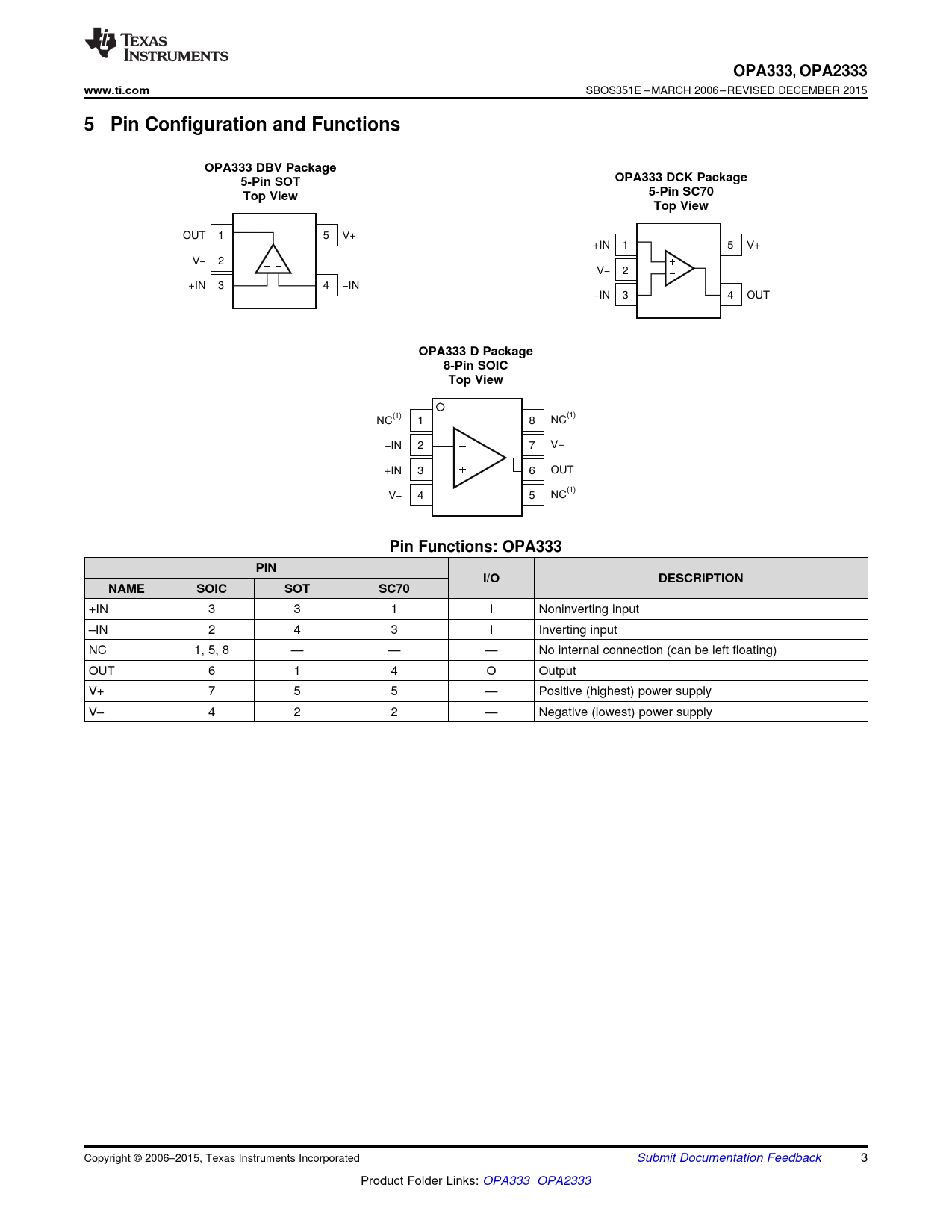
OPA333,. OPA2333. www.ti.com. 5 Pin Configuration and Functions. OPA333 DBV Package. OPA333 DCK Package. 5-Pin SOT. 5-Pin SC70
70 предложений от 27 поставщиков Микросхема Операционный усилитель, TEXAS INSTRUMENTS OPA333AIDBVR Operational Amplifier, Zero-Drift, 1 Amplifier, 350kHz, 0.16V/µs, ± 0.9V to ± 2.75V, 1.8V to 5.5V... |
| OPA333AIDBVR
| 36 ₽ | |
| OPA333AIDBVR
Texas Instruments | 102 ₽ | |
| OPA333AIDBVR
| по запросу | |
| OPA333AIDBVR
Texas Instruments | по запросу | |
Модельный ряд для этого даташита
Текстовая версия документа
OPA333, OPA2333 www.ti.com
SBOS351E – MARCH 2006 – REVISED DECEMBER 2015
5 Pin Configuration and Functions OPA333 DBV Package OPA333 DCK Package 5-Pin SOT 5-Pin SC70 Top View Top View
OUT 1 5 V+ +IN 1 5 V+ V 2 - V 2 - +IN 3 4 IN - IN 3 4 OUT -
OPA333 D Package 8-Pin SOIC Top View
(1) (1) NC 1 8 NC 2 7 V+ -IN +IN 3 6 OUT (1) V 4 5 NC -
Pin Functions: OPA333 PIN I/O DESCRIPTION NAME SOIC SOT SC70
+IN 3 3 1 I Noninverting input –IN 2 4 3 I Inverting input NC 1, 5, 8 — — — No internal connection (can be left floating) OUT 6 1 4 O Output V+ 7 5 5 — Positive (highest) power supply V– 4 2 2 — Negative (lowest) power supply Copyright © 2006–2015, Texas Instruments Incorporated Submit Documentation Feedback 3 Product Folder Links: OPA333 OPA2333 Document Outline 1 Features 2 Applications 3 Description Table of Contents 4 Revision History 5 Pin Configuration and Functions 6 Specifications 6.1 Absolute Maximum Ratings 6.2 ESD Ratings 6.3 Recommended Operating Conditions 6.4 Thermal Information: OPA333 6.5 Thermal Information: OPA2333 6.6 Electrical Characteristics 6.7 Typical Characteristics 7 Detailed Description 7.1 Overview 7.2 Functional Block Diagram 7.3 Feature Description 7.3.1 Operating Voltage 7.3.2 Input Voltage 7.3.3 Internal Offset Correction 7.3.4 Achieving Output Swing to the Op Amp Negative Rail 7.3.5 DFN Package 7.4 Device Functional Modes 8 Application and Implementation 8.1 Application Information 8.2 Typical Applications 8.2.1 High-Side Voltage-to-Current (V-I) Converter 8.2.1.1 Design Requirements 8.2.1.2 Detailed Design Procedure 8.2.1.3 Application Curve 8.2.2 Precision, Low-Level Voltage-to-Current (V-I) Converter 8.2.2.1 Design Requirements 8.2.2.2 Detailed Design Procedure 8.2.2.3 Application Curves 8.2.3 Composite Amplifier 8.2.3.1 Design Requirements 8.2.3.2 Detailed Design Procedure 8.2.3.3 Application Curve 8.3 System Examples 8.3.1 Temperature Measurement Application 8.3.2 Single Operational Amplifier Bridge Amplifier Application 8.3.3 Low-Side Current Monitor Application 8.3.4 Other Applications 9 Power Supply Recommendations 10 Layout 10.1 Layout Guidelines 10.1.1 General Layout Guidelines 10.1.2 DFN Layout Guidelines 10.2 Layout Example 11 Device and Documentation Support 11.1 Device Support 11.1.1 Development Support 11.2 Documentation Support 11.2.1 Related Documentation 11.3 Related Links 11.4 Community Resources 11.5 Trademarks 11.6 Electrostatic Discharge Caution 11.7 Glossary 12 Mechanical, Packaging, and Orderable Information

 Купить OPA333AIDBVR на РадиоЛоцман.Цены — от 29 до 344 ₽


