Datasheet FT232R (FTDI) - 7
| Производитель | FTDI |
| Описание | USB UART IC |
| Страниц / Страница | 47 / 7 — Document No.: FT_000053. FT232R USB UART IC Datasheet Version 2.11. … |
| Версия | 2.11 |
| Формат / Размер файла | PDF / 833 Кб |
| Язык документа | английский |
Document No.: FT_000053. FT232R USB UART IC Datasheet Version 2.11. Clearance No.: FTDI# 38

Текстовая версия документа
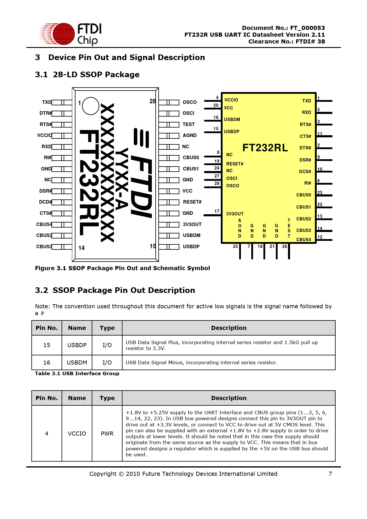
Document No.: FT_000053 FT232R USB UART IC Datasheet Version 2.11 Clearance No.: FTDI# 38 3 Device Pin Out and Signal Description 3.1 28-LD SSOP Package 4 1 TXD 28 OSCO VCCIO 1 TXD 20 VCC 5 X DTR# OSCI RXD 16 USBDM 3 F X RTS# TEST RTS# 15 USBDP X VCCIO AGND 11 CTS# T XY RXD NC FT232RL 2 XY F DTR# 8 2 NC RI# CBUS0 9 19 DSR# RESET# 3 X T GND CBUS1 24 NC 10 DCD# 27 X NC GND OSCI 6 2 X- D 28 RI# OSCO DSR# VCC 23 X CBUS0 R A DCD# RESET# X I 22 CBUS1 CTS# GND 17 3V3OUT L 13 X A T CBUS2 CBUS4 3V3OUT G G G G E X 14 N N N N S CBUS3 CBUS2 USBDM D D D D T 12 CBUS4 X CBUS3 USBDP 14 15 25 7 18 21 26 Figure 3.1 SSOP Package Pin Out and Schematic Symbol 3.2 SSOP Package Pin Out Description
Note: The convention used throughout this document for active low signals is the signal name followed by a #
Pin No. Name Type Description
15 USBDP I/O USB Data Signal Plus, incorporating internal series resistor and 1.5kΩ pull up resistor to 3.3V. 16 USBDM I/O USB Data Signal Minus, incorporating internal series resistor.
Table 3.1 USB Interface Group Pin No. Name Type Description
+1.8V to +5.25V supply to the UART Interface and CBUS group pins (1...3, 5, 6, 9...14, 22, 23). In USB bus powered designs connect this pin to 3V3OUT pin to drive out at +3.3V levels, or connect to VCC to drive out at 5V CMOS level. This 4 VCCIO PWR pin can also be supplied with an external +1.8V to +2.8V supply in order to drive outputs at lower levels. It should be noted that in this case this supply should originate from the same source as the supply to VCC. This means that in bus powered designs a regulator which is supplied by the +5V on the USB bus should be used. Copyright © 2010 Future Technology Devices International Limited 7 Document Outline 1 Typical Applications 1.1 Driver Support 1.2 Part Numbers Note: Packing codes for xxxx is: 1.1 1.1 1.3 USB Compliant 2 FT232R Block Diagram 3 Device Pin Out and Signal Description 3.1 28-LD SSOP Package 3.2 SSOP Package Pin Out Description 3.3 QFN-32 Package 3.4 QFN-32 Package Signal Description 3.5 CBUS Signal Options 4 Function Description 4.1 Key Features 4.2 Functional Block Descriptions 5 Devices Characteristics and Ratings 5.1 Absolute Maximum Ratings 5.2 DC Characteristics 5.3 EEPROM Reliability Characteristics 5.4 Internal Clock Characteristics 5.5 Thermal Characteristics 6 USB Power Configurations 6.1 USB Bus Powered Configuration 1.1 1.1 6.2 Self Powered Configuration 6.3 USB Bus Powered with Power Switching Configuration 6.4 USB Bus Powered with Selectable External Logic Supply 7 Application Examples 7.1 USB to RS232 Converter 7.2 USB to RS485 Coverter 1.1 1.1 1.1 7.3 USB to RS422 Converter 7.4 USB to MCU UART Interface 1.1 1.1 1.1 7.5 LED Interface 7.6 Using the External Oscillator 8 Internal EEPROM Configuration 9 Package Parameters 9.1 SSOP-28 Package Dimensions 9.2 QFN-32 Package Dimensions 9.3 QFN-32 Package Typical Pad Layout 1.1 9.4 QFN-32 Package Typical Solder Paste Diagram 9.5 Solder Reflow Profile 10 Alternative Parts 11 Contact Information Appendix A – References Appendix B - List of Figures and Tables Appendix C - Revision History