Datasheet AD8338 (Analog Devices)
| Производитель | Analog Devices |
| Описание | Low Power, 18 MHz Variable Gain Amplifier |
| Страниц / Страница | 20 / 1 — Low Power, 18 MHz Variable Gain Amplifier. Data Sheet. AD8338. FEATURES. … |
| Версия | B |
| Формат / Размер файла | PDF / 483 Кб |
| Язык документа | английский |
Low Power, 18 MHz Variable Gain Amplifier. Data Sheet. AD8338. FEATURES. FUNCTIONAL BLOCK DIAGRAM

19 предложений от 8 поставщиков Интегральные микросхемы Аналоговая техника — усилители — инструменты, ОУ (операционные), буферные |
| AD8338ACPZ-RL
Analog Devices | 400 ₽ | |
| AD8338ACPZ-RL
Analog Devices | 421 ₽ | |
| AD8338ACPZ-RL
Analog Devices | от 1 674 ₽ | |
| AD8338ACPZ-RL
Analog Devices | по запросу | |
Модельный ряд для этого даташита
Текстовая версия документа
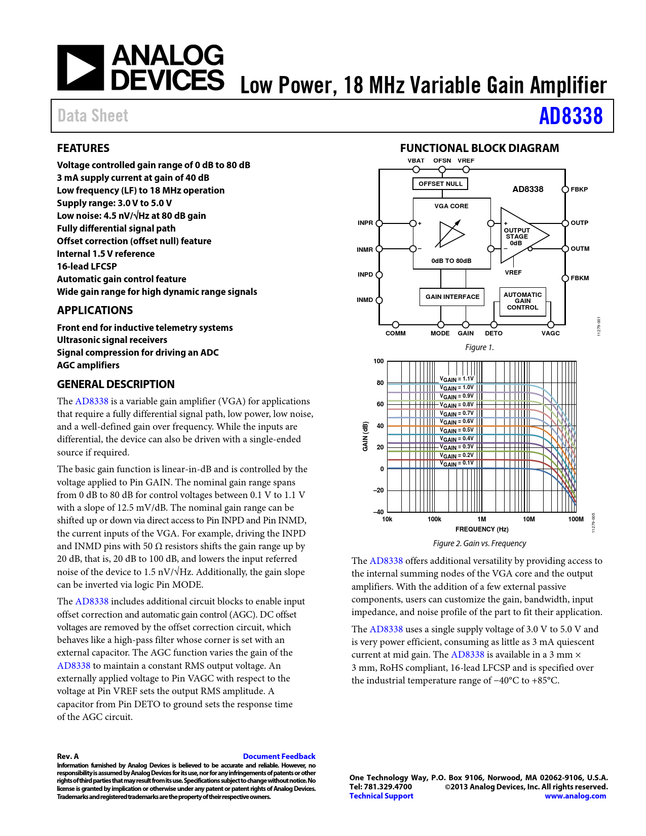
Low Power, 18 MHz Variable Gain Amplifier Data Sheet AD8338 FEATURES FUNCTIONAL BLOCK DIAGRAM Voltage controlled gain range of 0 dB to 80 dB VBAT OFSN VREF 3 mA supply current at gain of 40 dB OFFSET NULL Low frequency (LF) to 18 MHz operation AD8338 FBKP Supply range: 3.0 V to 5.0 V VGA CORE Low noise: 4.5 nV/
√
Hz at 80 dB gain Fully differential signal path INPR + + OUTP OUTPUT Offset correction (offset null) feature STAGE 0dB Internal 1.5 V reference INMR – – OUTM 16-lead LFCSP 0dB TO 80dB VREF Automatic gain control feature INPD FBKM Wide gain range for high dynamic range signals AUTOMATIC GAIN INTERFACE INMD GAIN APPLICATIONS CONTROL Front end for inductive telemetry systems
001
COMM MODE GAIN DETO VAGC Ultrasonic signal receivers
11279- Figure 1.
Signal compression for driving an ADC AGC amplifiers 100 GENERAL DESCRIPTION V 80 GAIN = 1.1V VGAIN = 1.0V
The AD8338 is a variable gain amplifier (VGA) for applications
VGAIN = 0.9V 60 VGAIN = 0.8V
that require a fully differential signal path, low power, low noise,
VGAIN = 0.7V
and a wel -defined gain over frequency. While the inputs are
VGAIN = 0.6V B) 40 d VGAIN = 0.5V
differential, the device can also be driven with a single-ended
N ( VGAIN = 0.4V AI
source if required.
20 V G GAIN = 0.3V VGAIN = 0.2V
The basic gain function is linear-in-dB and is controlled by the
VGAIN = 0.1V 0
voltage applied to Pin GAIN. The nominal gain range spans from 0 dB to 80 dB for control voltages between 0.1 V to 1.1 V
–20
with a slope of 12.5 mV/dB. The nominal gain range can be
–40
shifted up or down via direct access to Pin INPD and Pin INMD,
10k 100k 1M 10M 100M
005 the current inputs of the VGA. For example, driving the INPD
FREQUENCY (Hz)
1279- 1 and INMD pins with 50 Ω resistors shifts the gain range up by Figure 2. Gain vs. Frequency 20 dB, that is, 20 dB to 100 dB, and lowers the input referred The AD8338 offers additional versatility by providing access to noise of the device to 1.5 nV/√Hz. Additionally, the gain slope the internal summing nodes of the VGA core and the output can be inverted via logic Pin MODE. amplifiers. With the addition of a few external passive The AD8338 includes additional circuit blocks to enable input components, users can customize the gain, bandwidth, input offset correction and automatic gain control (AGC). DC offset impedance, and noise profile of the part to fit their application. voltages are removed by the offset correction circuit, which The AD8338 uses a single supply voltage of 3.0 V to 5.0 V and behaves like a high-pass filter whose corner is set with an is very power efficient, consuming as little as 3 mA quiescent external capacitor. The AGC function varies the gain of the current at mid gain. The AD8338 is available in a 3 mm × AD8338 to maintain a constant RMS output voltage. An 3 mm, RoHS compliant, 16-lead LFCSP and is specified over external y applied voltage to Pin VAGC with respect to the the industrial temperature range of −40°C to +85°C. voltage at Pin VREF sets the output RMS amplitude. A capacitor from Pin DETO to ground sets the response time of the AGC circuit.
Rev. A Document Feedback Information furnished by Analog Devices is believed to be accurate and reliable. However, no responsibility is assumed by Analog Devices for its use, nor for any infringements of patents or other rights of third parties that may result from its use. Specifications subject to change without notice. No One Technology Way, P.O. Box 9106, Norwood, MA 02062-9106, U.S.A. license is granted by implication or otherwise under any patent or patent rights of Analog Devices. Tel: 781.329.4700 ©2013 Analog Devices, Inc. All rights reserved. Trademarks and registered trademarks are the property of their respective owners. Technical Support www.analog.com
Document Outline Features Applications General Description Functional Block Diagram Revision History Specifications AC Specifications Absolute Maximum Ratings Thermal Resistance ESD Caution Pin Configuration and Function Descriptions Typical Performance Characteristics Theory of Operation Introduction Overall Structure of the AD8338 VGA Core Normal Operating Conditions INPR, INMR, INPD, and INMD Pins FBKP, FBKM, OUTP, and OUTM Pins Linear-in-dB Gain Control, GAIN Pin Inversion of the Gain Slope, MODE Pin Offset Correction Circuit, OFSN Pin AGC Circuit, VAGC Pin Internal Reference, Pin VREF Explanation of the Gain Function Effects of Using External Resistors Adjusting The Output Common-Mode Voltage Applications Information Simple On-Off Keyed (OOK) Receiver Interfacing the AD8338 to an ADC Outline Dimensions Ordering Guide

 Купить AD8338ACPZ-RL на РадиоЛоцман.Цены — от 400 до 1 674 ₽