Datasheet MC74AC125, MC74ACT125 (ON Semiconductor) - 6
| Производитель | ON Semiconductor |
| Описание | Quad 3-State Buffer with Low Enable |
| Страниц / Страница | 9 / 6 — PACKAGE DIMENSIONS. SOIC−14 NB. SCALE 1:1. DETAIL A. MILLIMETERS. INCHES. … |
| Формат / Размер файла | PDF / 245 Кб |
| Язык документа | английский |
PACKAGE DIMENSIONS. SOIC−14 NB. SCALE 1:1. DETAIL A. MILLIMETERS. INCHES. DIM. MIN. MAX. 13X b. X 45. C SEATING. PLANE. GENERIC
40 предложений от 22 поставщиков Интегральные микросхемы Логические микросхемы - Буферы, Приемники, Приемопередатчики |
| MC74AC125DG
ON Semiconductor | 6.24 ₽ | |
| MC74AC125DG
ON Semiconductor | 12 ₽ | |
| MC74AC125DG
ON Semiconductor | 67 ₽ | |
| MC74AC125DG
ON Semiconductor | по запросу | |
Модельный ряд для этого даташита
Текстовая версия документа
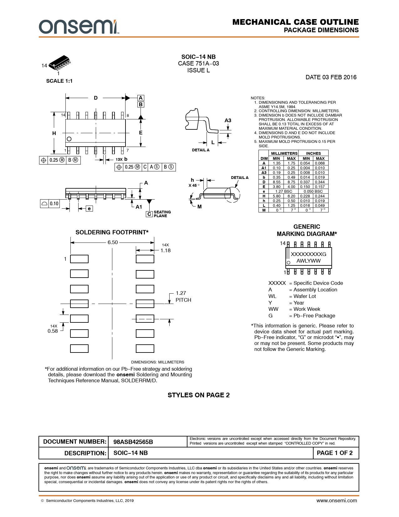
MECHANICAL CASE OUTLINE
PACKAGE DIMENSIONS SOIC−14 NB
CASE 751A−03 14 ISSUE L 1 DATE 03 FEB 2016
SCALE 1:1 D A
NOTES: 1. DIMENSIONING AND TOLERANCING PER
B
ASME Y14.5M, 1994. 2. CONTROLLING DIMENSION: MILLIMETERS. 14 8 3. DIMENSION b DOES NOT INCLUDE DAMBAR PROTRUSION. ALLOWABLE PROTRUSION
A3
SHALL BE 0.13 TOTAL IN EXCESS OF AT MAXIMUM MATERIAL CONDITION.
E
4. DIMENSIONS D AND E DO NOT INCLUDE
H
MOLD PROTRUSIONS. 5. MAXIMUM MOLD PROTRUSION 0.15 PER
L
SIDE. 1 7
DETAIL A MILLIMETERS INCHES
0.25
DIM MIN MAX MIN MAX
M B M
13X b A
1.35 1.75 0.054 0.068 0.25 M C A S B S
A1
0.10 0.25 0.004 0.010
A3
0.19 0.25 0.008 0.010
h DETAIL A b
0.35 0.49 0.014 0.019
A D
8.55 8.75 0.337 0.344
X 45
_
E
3.80 4.00 0.150 0.157
e
1.27 BSC 0.050 BSC
H
5.80 6.20 0.228 0.244
h
0.25 0.50 0.010 0.019 0.10
A1 M L
0.40 1.25 0.016 0.049
e M
0 _ 7 _ 0 _ 7 _
C SEATING PLANE GENERIC SOLDERING FOOTPRINT* MARKING DIAGRAM*
6.50 14X 14 1.18 XXXXXXXXXG 1 AWLYWW 1 XXXXX = Specific Device Code A = Assembly Location 1.27 WL = Wafer Lot PITCH Y = Year WW = Work Week G = Pb−Free Package 14X *This information is generic. Please refer to 0.58 device data sheet for actual part marking. Pb−Free indicator, “G” or microdot “G”, may or may not be present. Some products may not follow the Generic Marking. DIMENSIONS: MILLIMETERS *For additional information on our Pb−Free strategy and soldering details, please download the
onsemi
Soldering and Mounting Techniques Reference Manual, SOLDERRM/D.
STYLES ON PAGE 2 DOCUMENT NUMBER: 98ASB42565B
Electronic versions are uncontrolled except when accessed directly from the Document Repository. Printed versions are uncontrolled except when stamped “CONTROLLED COPY” in red.
DESCRIPTION: SOIC−14 NB PAGE 1 OF 2 onsemi
and are trademarks of Semiconductor Components Industries, LLC dba
onsemi
or its subsidiaries in the United States and/or other countries.
onsemi
reserves the right to make changes without further notice to any products herein.
onsemi
makes no warranty, representation or guarantee regarding the suitability of its products for any particular purpose, nor does
onsemi
assume any liability arising out of the application or use of any product or circuit, and specifically disclaims any and all liability, including without limitation special, consequential or incidental damages.
onsemi
does not convey any license under its patent rights nor the rights of others. © Semiconductor Components Industries, LLC, 2019 www.onsemi.com

 Купить MC74AC125DG на РадиоЛоцман.Цены — от 6.24 до 471 ₽


