Datasheet TLR377GYZ (Rohm) - 5
| Производитель | Rohm |
| Описание | Ultra Small Package & High Precision Rail-to-Rail Input/Output CMOS Operational Amplifier |
| Страниц / Страница | 23 / 5 — TLR377GYZ. Electrical Characteristics - continued |
| Формат / Размер файла | PDF / 1.2 Мб |
| Язык документа | английский |
TLR377GYZ. Electrical Characteristics - continued

Модельный ряд для этого даташита
Текстовая версия документа
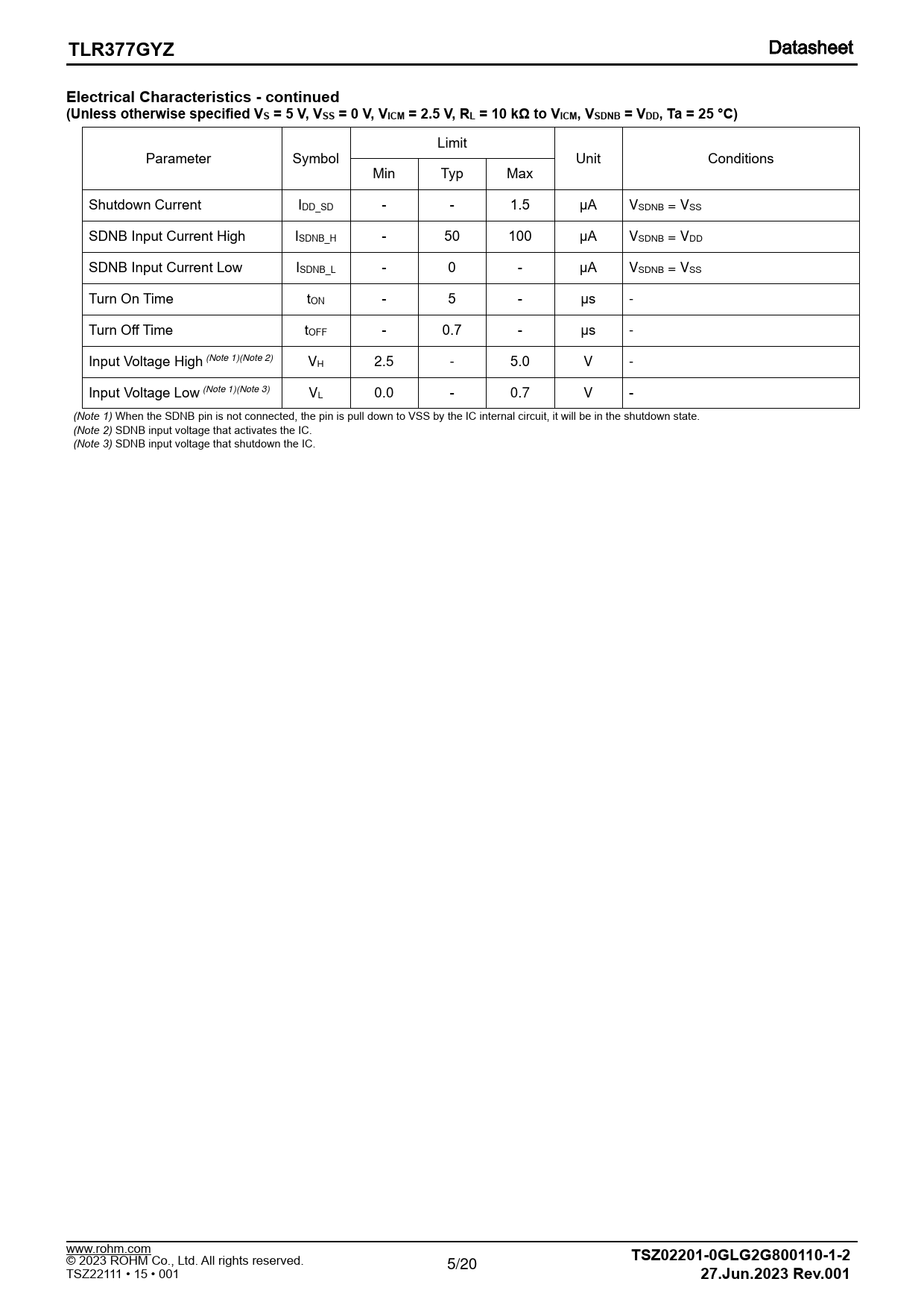
TLR377GYZ Electrical Characteristics - continued (Unless otherwise specified VS = 5 V, VSS = 0 V, VICM = 2.5 V, RL = 10 kΩ to VICM, VSDNB = VDD, Ta = 25 °C)
Limit Parameter Symbol Unit Conditions Min Typ Max Shutdown Current IDD_SD - - 1.5 μA VSDNB = VSS SDNB Input Current High ISDNB_H - 50 100 μA VSDNB = VDD SDNB Input Current Low ISDNB_L - 0 - μA VSDNB = VSS Turn On Time tON - 5 - μs - Turn Off Time tOFF - 0.7 - μs - Input Voltage High (Note 1)(Note 2) VH 2.5 - 5.0 V - Input Voltage Low (Note 1)(Note 3) VL 0.0 - 0.7 V - (Note 1) When the SDNB pin is not connected, the pin is pull down to VSS by the IC internal circuit, it will be in the shutdown state. (Note 2) SDNB input voltage that activates the IC. (Note 3) SDNB input voltage that shutdown the IC. www.rohm.com
TSZ02201-0GLG2G800110-1-2
© 2023 ROHM Co., Ltd. All rights reserved. 5 /20 TSZ22111 • 15 • 001
27.Jun.2023 Rev.001
Document Outline General Description Features Applications Key Specifications Package Typical Application Circuit Pin Configuration Pin Description Block Diagram Description of Blocks Absolute Maximum Ratings Thermal Resistance Recommended Operating Conditions Electrical Characteristics Typical Performance Curves Figure 1. Supply Current vs Supply Voltage Figure 2. Supply Current vs Ambient Temperature Figure 3. Output Voltage High vs Supply Voltage Figure 4. Output Voltage High vs Ambient Temperature Figure 5. Output Voltage Low vs Supply Voltage Figure 6. Output Voltage Low vs Ambient Temperature Figure 7. Output Source Current vs Output Voltage Figure 8. Output Sink Current vs Output Voltage Figure 9. Input Offset Voltage vs Supply Voltage Figure 10. Input Offset Voltage vs Ambient Temperature Figure 11. Input Offset Voltage vs Input Common-mode Voltage Figure 12. Large Signal Voltage Gain vs Supply Voltage Figure 13. Large Signal Voltage Gain vs Ambient Temperature Figure 14. Common-mode Rejection Ratio vs Supply Voltage Figure 15. Common-mode Rejection Ratio vs Ambient Temperature Figure 16. Power Supply Rejection Ratio vs Ambient Temperature Figure 17. Input Bias Current vs Ambient Temperature Figure 18. Input-referred Noise Voltage Density vs Frequency Figure 19. Slew Rate vs Supply Voltage Figure 20. Slew Rate vs Ambient Temperature Figure 21. Gain Bandwidth Product vs Ambient Temperature Figure 22. Phase Margin vs Load Capacitance Figure 23. Voltage Gain, Phase vs Frequency Figure 24. Voltage Gain vs Frequency Figure 25. Turn On Time vs Ambient Temperature Figure 26. Turn Off Time vs Ambient Temperature Figure 27. Shutdown Current vs Ambient Temperature Figure 28. Output Voltage vs SDNB Voltage Application Information Application Examples I/O Equivalence Circuits Operational Notes 1. Reverse Connection of Power Supply 2. Power Supply Lines 3. Ground Voltage 4. Ground Wiring Pattern 5. Recommended Operating Conditions 6. Inrush Current 7. Testing on Application Boards 8. Inter-pin Short and Mounting Errors 9. Unused Input Pins 10. Regarding the Input Pin of the IC 11. Ceramic Capacitor 12. Disturbance Light Ordering Information Marking Diagram Physical Dimension and Packing Information Revision History
