DatasheetsDatasheet MTP50P03HDLG (ON Semiconductor)
Datasheet MTP50P03HDLG (ON Semiconductor)
| Производитель | ON Semiconductor |
| Описание | Power MOSFET 50 Amps, 30 Volts, Logic Level P−Channel TO−220 |
| Страниц / Страница | 8 / 1 — 50 Amps, 30 Volts, Logic Level P−Channel TO−220. www.onsemi.com. 50 … |
| Формат / Размер файла | PDF / 113 Кб |
| Язык документа | английский |
50 Amps, 30 Volts, Logic Level P−Channel TO−220. www.onsemi.com. 50 AMPERES, 30 VOLTS. DS(on) = 25 m. P−Channel. Features

18 предложений от 14 поставщиков Дискретные полупроводники Транзисторы — полевые — одиночные |
| MTP50P03HDL
ON Semiconductor | 50 ₽ | |
| MTP50P03HDL
ON Semiconductor | от 52 ₽ | |
| MTP50P03HDL
ON Semiconductor | от 431 ₽ | |
| MTP50P03HDL
ON Semiconductor | от 907 ₽ | |
Модельный ряд для этого даташита
Текстовая версия документа
MTP50P03HDLG Power MOSFET
50 Amps, 30 Volts, Logic Level P−Channel TO−220
This Power MOSFET is designed to withstand high energy in the avalanche and commutation modes. The energy efficient design also offers a drain−to−source diode with a fast recovery time. Designed for
www.onsemi.com
low voltage, high speed switching applications in power supplies, converters and PWM motor controls, these devices are particularly
50 AMPERES, 30 VOLTS
well suited for bridge circuits where diode speed and commutating
R
safe operating areas are critical and offer additional safety margin
DS(on) = 25 m
W against unexpected voltage transients.
P−Channel Features
• D Avalanche Energy Specified • Source−to−Drain Diode Recovery Time Comparable to a Discrete Fast Recovery Diode • Diode is Characterized for Use in Bridge Circuits G • IDSS and VDS(on) Specified at Elevated Temperature • These are Pb−Free Devices* S
MAXIMUM RATINGS
(T
MARKING DIAGRAM
C = 25°C unless otherwise noted)
& PIN ASSIGNMENT Rating Symbol Value Unit
4 Drain−Source Voltage VDSS 30 Vdc Drain Drain−Gate Voltage (R 4 GS = 1.0 MW) VDGR 30 Vdc Gate−Source Voltage − Continuous VGS ± 15 Vdc − Non−Repetitive (tp ≤ 10 ms) VGSM ± 20 Vpk
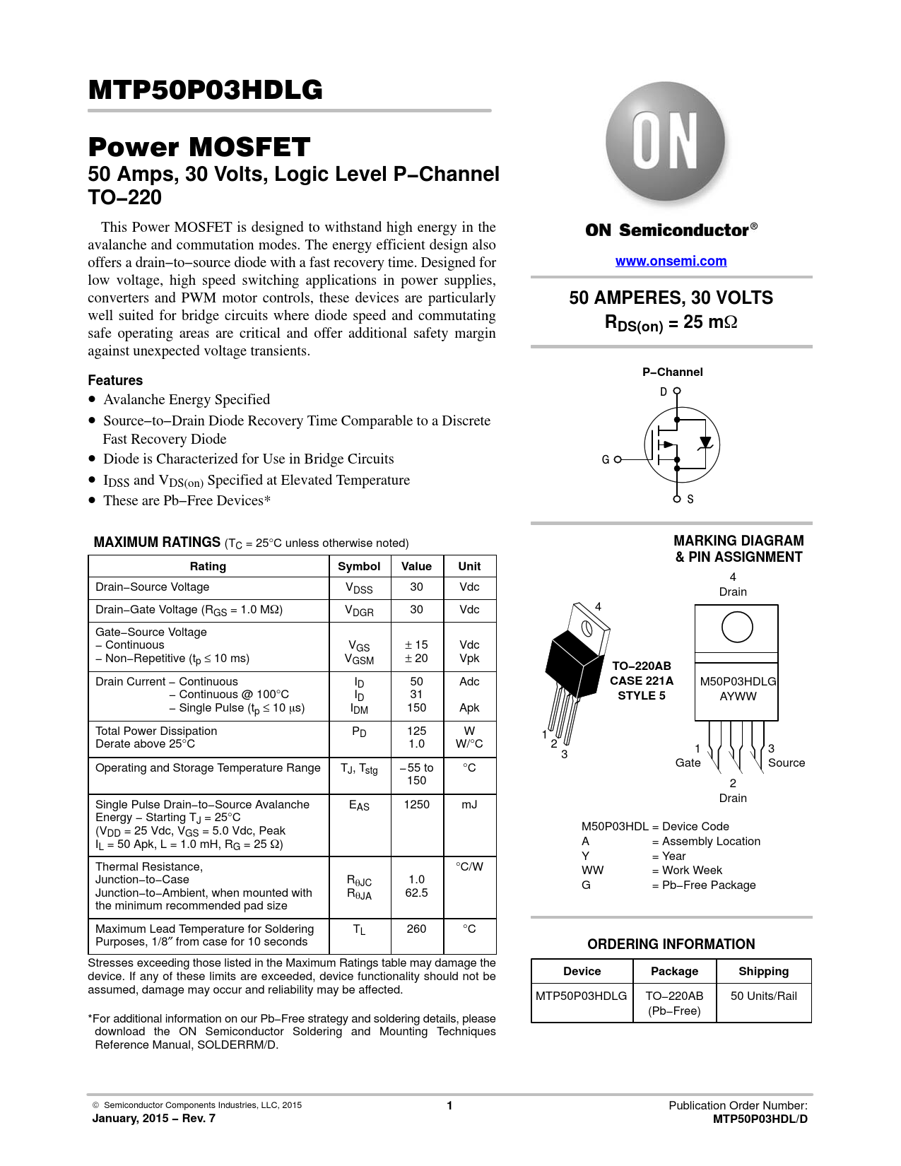
TO−220AB
Drain Current − Continuous ID 50 Adc
CASE 221A
M50P03HDLG Drain Current − Continuous @ 100°C ID 31
STYLE 5
AYWW Drain Current − Single Pulse (tp ≤ 10 ms) IDM 150 Apk Total Power Dissipation PD 125 W 1 Derate above 25°C 1.0 W/°C 2 1 3 3 Operating and Storage Temperature Range T Gate Source J, Tstg − 55 to °C 150 2 Drain Single Pulse Drain−to−Source Avalanche EAS 1250 mJ Energy − Starting TJ = 25°C (V M50P03HDL = Device Code DD = 25 Vdc, VGS = 5.0 Vdc, Peak I A = Assembly Location L = 50 Apk, L = 1.0 mH, RG = 25 W) Y = Year Thermal Resistance, °C/W WW = Work Week Junction−to−Case RqJC 1.0 G = Pb−Free Package Junction−to−Ambient, when mounted with RqJA 62.5 the minimum recommended pad size Maximum Lead Temperature for Soldering TL 260 °C Purposes, 1/8″ from case for 10 seconds
ORDERING INFORMATION
Stresses exceeding those listed in the Maximum Ratings table may damage the device. If any of these limits are exceeded, device functionality should not be
Device Package Shipping
assumed, damage may occur and reliability may be affected. MTP50P03HDLG TO−220AB 50 Units/Rail (Pb−Free) *For additional information on our Pb−Free strategy and soldering details, please download the ON Semiconductor Soldering and Mounting Techniques Reference Manual, SOLDERRM/D. © Semiconductor Components Industries, LLC, 2015
1
Publication Order Number:
January, 2015 − Rev. 7 MTP50P03HDL/D

 Купить MTP50P03HDL на РадиоЛоцман.Цены — от 50 до 966 ₽