Datasheet LMR1901YG-M (Rohm) - 8
| Производитель | Rohm |
| Описание | Automotive Ultra Low Power Low Offset Voltage Rail-to-Rail Input/Output CMOS Operational Amplifiers |
| Страниц / Страница | 24 / 8 — LMR1901YG-M. Typical Performance Curves - continued. … |
| Формат / Размер файла | PDF / 2.1 Мб |
| Язык документа | английский |
LMR1901YG-M. Typical Performance Curves - continued. TSZ02201-0GLG2G800170-1-2. 04.Aug.2023 Rev.001

Модельный ряд для этого даташита
Текстовая версия документа
link to page 4
LMR1901YG-M Typical Performance Curves - continued
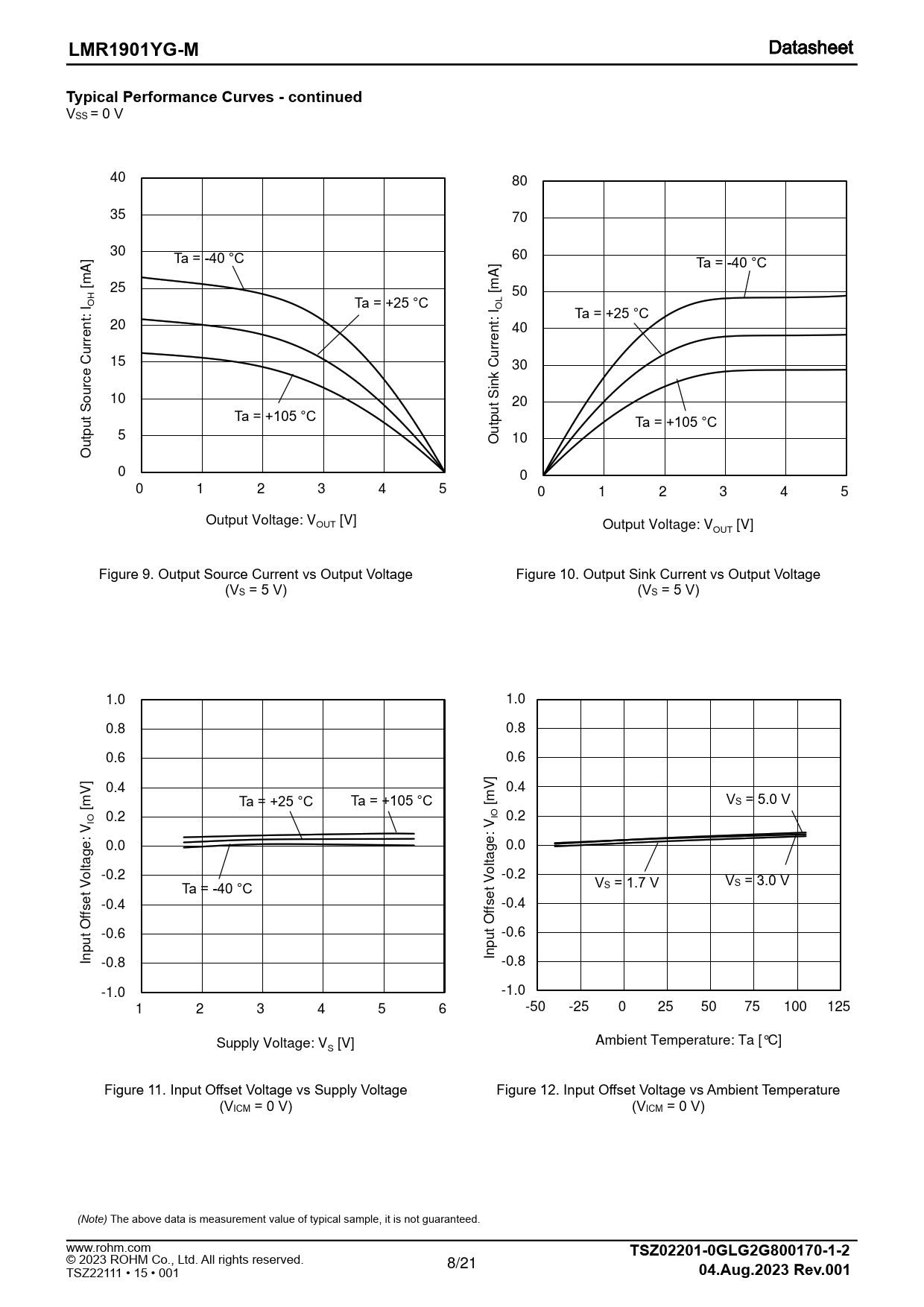
VSS = 0 V 40 80 35 70 30 60 Ta = -40 °C A] Ta = -40 °C A] [m 25 [m 50 I OH Ta = +25 °C I OL t: Ta = +25 °C n 20 nt 40 urre Curre 15 C e 30 k rc u 10 Sin So t 20 t Ta = +105 °C u pu Ta = +105 °C tp 5 ut u O 10 O 0 0 0 1 2 3 4 5 0 1 2 3 4 5 Output Voltage: V [V] OUT Output Voltage: V [V] OUT Figure 9. Output Source Current vs Output Voltage Figure 10. Output Sink Current vs Output Voltage (VS = 5 V) (VS = 5 V) 1.0 1.0 Ta = -40 °C 0.8 0.8 0.6 0.6 Ta = +25 °C V] 0.4 V] 0.4 m m V [ Ta = +25 °C Ta = +105 °C [ S = 5.0 V IO 0.2 IO 0.2 V V : e e 0.0 g 0.0 g ta ta l Ta = +125 °C l -0.2 -0.2 Vo Vo VS = 1.7 V VS = 3.0 V t Ta = -40 °C t e e s -0.4 s -0.4 ff ff O O t -0.6 t -0.6 u u p p In In -0.8 -0.8 -1.0 -1.0 1 2 3 4 5 6 -50 -25 0 25 50 75 100 125 Supply Voltage: V [V] Ambient Temperature: Ta [°C] S Figure 11. Input Offset Voltage vs Supply Voltage Figure 12. Input Offset Voltage vs Ambient Temperature (VICM = 0 V) (VICM = 0 V) (Note) The above data is measurement value of typical sample, it is not guaranteed. www.rohm.com
TSZ02201-0GLG2G800170-1-2
8 © 2023 ROHM Co., Ltd. All rights reserved. /21 TSZ22111 • 15 • 001
04.Aug.2023 Rev.001
Document Outline General Description Features Applications Key Specifications Package Typical Application Circuit Pin Configuration Block Diagram Description of Blocks Absolute Maximum Ratings Thermal Resistance Recommended Operating Conditions Function Explanation Electrical Characteristics Typical Performance Curves Figure 1. Supply Current vs Supply Voltage Figure 2. Supply Current vs Ambient Temperature Figure 3. Output Voltage High vs Supply Voltage Figure 4. Output Voltage High vs Ambient Temperature Figure 5. Output Voltage Low vs Supply Voltage Figure 6. Output Voltage Low vs Ambient Temperature Figure 7. Output Source Current vs Output Voltage Figure 8. Output Sink Current vs Output Voltage Figure 9. Output Source Current vs Output Voltage Figure 10. Output Sink Current vs Output Voltage Figure 11. Input Offset Voltage vs Supply Voltage Figure 12. Input Offset Voltage vs Ambient Temperature Figure 13. Input Offset Voltage vs Supply Voltage Figure 14. Input Offset Voltage vs Ambient Temperature Figure 15. Input Offset Voltage vs Common-mode Input Voltage Figure 16. Input Offset Voltage vs Common-mode Input Voltage Figure 17. Large Signal Voltage Gain vs Supply Voltage Figure 18. Large Signal Voltage Gain vs Ambient Temperature Figure 19. Common-mode Rejection Ratio vs Supply Voltage Figure 20. Common-mode Rejection Ratio vs Ambient Temperature Figure 21. Power Supply Rejection Ratio vs Ambient Temperature Figure 22. Input Bias Current vs Ambient Temperature Figure 23. Input-referred Noise Voltage Density vs Frequency Figure 24. Input-referred Noise Voltage Density vs Frequency Figure 25. Slew Rate vs Supply Voltage Figure 26. Slew Rate vs Ambient Temperature Figure 27. Slew Rate vs Ambient Temperature Figure 28. Gain Bandwidth Product vs Ambient Temperature Figure 29. Phase Margin vs Load Capacitance Figure 30. Phase Margin vs Load Capacitance Figure 31. Voltage Gain, Phase vs Frequency Figure 32. Voltage Gain, Phase vs Frequency Figure 33. Large-Signal Step Response Figure 34. Large-Signal Step Response Application Examples I/O Equivalence Circuits Operational Notes 1. Reverse Connection of Power Supply 2. Power Supply Lines 3. Ground Voltage 4. Ground Wiring Pattern 5. Recommended Operating Conditions 6. Inrush Current 7. Testing on Application Boards 8. Inter-pin Short and Mounting Errors 9. Unused Input Pins 10. Regarding the Input Pin of the IC 11. Ceramic Capacitor Ordering Information Marking Diagram Physical Dimension and Packing Information Revision History
