Datasheet MCP1502 (Microchip)
| Производитель | Microchip |
| Описание | High-Precision Buffered Voltage Reference |
| Страниц / Страница | 28 / 1 — MCP1502. High-Precision Buffered Voltage Reference. Features. General … |
| Формат / Размер файла | PDF / 19.5 Мб |
| Язык документа | английский |
MCP1502. High-Precision Buffered Voltage Reference. Features. General Description. Package Types. Applications. Related Parts

Текстовая версия документа
MCP1502 High-Precision Buffered Voltage Reference Features General Description
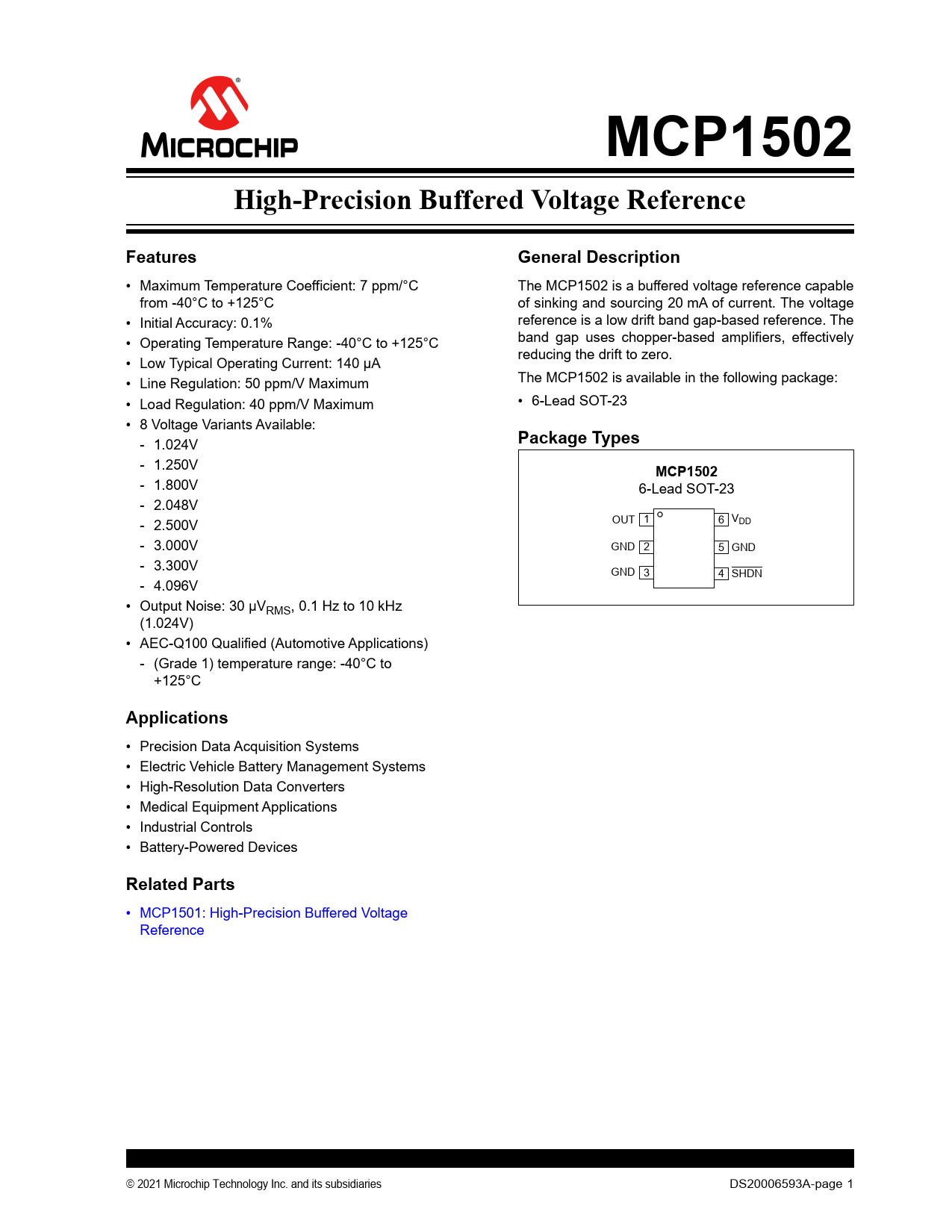
• Maximum Temperature Coefficient: 7 ppm/°C The MCP1502 is a buffered voltage reference capable from -40°C to +125°C of sinking and sourcing 20 mA of current. The voltage • Initial Accuracy: 0.1% reference is a low drift band gap-based reference. The • Operating Temperature Range: -40°C to +125°C band gap uses chopper-based amplifiers, effectively reducing the drift to zero. • Low Typical Operating Current: 140 µA • Line Regulation: 50 ppm/V Maximum The MCP1502 is available in the following package: • Load Regulation: 40 ppm/V Maximum • 6-Lead SOT-23 • 8 Voltage Variants Available: - 1.024V
Package Types
- 1.250V
MCP1502
- 1.800V 6-Lead SOT-23 - 2.048V - 2.500V OUT 1 6 VDD - 3.000V GND 2 5 GND - 3.300V GND 3 4 SHDN - 4.096V • Output Noise: 30 µVRMS, 0.1 Hz to 10 kHz (1.024V) • AEC-Q100 Qualified (Automotive Applications) - (Grade 1) temperature range: -40°C to +125°C
Applications
• Precision Data Acquisition Systems • Electric Vehicle Battery Management Systems • High-Resolution Data Converters • Medical Equipment Applications • Industrial Controls • Battery-Powered Devices
Related Parts
• MCP1501: High-Precision Buffered Voltage Reference 2021 Microchip Technology Inc. and its subsidiaries DS20006593A-page 1 Document Outline Features Applications Related Parts General Description Package Types Block Diagram 1.0 Pin Function Table TABLE 1-1: Pin Function Table 1.1 Buffered VREF Output (OUT) 1.2 System Ground (GND) 1.3 Shutdown Pin (SHDN) 1.4 Power Supply Input (VDD) 2.0 Electrical Characteristics Absolute Maximum Ratings(†) TABLE 2-1: DC Characteristics TABLE 2-2: Temperature Specifications 2.1 Terminology 2.1.1 Output Voltage (VOUT) 2.1.2 Input Voltage (VIN) 2.1.3 Temperature Coefficient (Tc) EQUATION 2-1: TC Calculation 2.1.4 Dropout Voltage (VDO) 2.1.5 Line Regulation EQUATION 2-2: EQUATION 2-3: EQUATION 2-4: EQUATION 2-5: EQUATION 2-6: 2.1.6 Load Regulation EQUATION 2-7: EQUATION 2-8: EQUATION 2-9: EQUATION 2-10: EQUATION 2-11: 2.1.7 Power Supply Rejection Ratio (PSRR) 2.1.8 Long-Term Drift 2.1.9 Output Voltage Hysteresis 2.1.10 Layout Consideration for Load Regulation 3.0 Typical Operating Curves FIGURE 3-1: MCP1502-10 VREF Output vs. Temperature, VDD = 5.5V. FIGURE 3-2: MCP1502-20 VREF Output vs. Temperature, VDD = 5.5V. FIGURE 3-3: MCP1502-40 VREF Output vs. Temperature, VDD = 5.5V. FIGURE 3-4: Load Regulation vs. Temperature. FIGURE 3-5: IDD vs. Temperature. FIGURE 3-6: MCP1502 – Line Regulation vs. Temperature. FIGURE 3-7: IDD vs. VDD for All Options. FIGURE 3-8: Noise vs. Frequency, No Load, TA = +25°C. FIGURE 3-9: PSRR vs. Frequency, No Load, TA = +25°C. FIGURE 3-10: PSRR vs. Frequency, 1 kΩ Load, TA = +25°C. FIGURE 3-11: Dropout Voltage vs. Load, TA = +25°C. FIGURE 3-12: MCP1502 Tempco Distribution, No Load, VDD = 2.7V. FIGURE 3-13: MCP1502 Tempco Distribution, No Load, VDD = 5.5V. FIGURE 3-14: VOUT Drift vs. Time, TA = +25°C, No Load, 800 Units. FIGURE 3-15: MCP1502-10 VREF and Load Regulation vs. Load Current. FIGURE 3-16: MCP1502-20 VREF and Load Regulation vs. Load Current. FIGURE 3-17: MCP1502-40 VREF and Load Regulation vs. Load Current. FIGURE 3-18: MCP1502 Output Voltage Histogram, VDD = 2.7V. FIGURE 3-19: MCP1502 Output Voltage Histogram, VDD = 5.5V. FIGURE 3-20: Fast Ramp Start-up @ +25°C for All Options. FIGURE 3-21: Slow Ramp Start-up @ +25°C for All Options. FIGURE 3-22: IDD Turn-On Transient Response. FIGURE 3-23: Shutdown Low-to-High Slow Ramp Turn-On Transient Response @ +25°C for All Options. FIGURE 3-24: Load Regulation Transient Response @ +25°C for All Options. FIGURE 3-25: Line Regulation Transient Response @ +25°C for All Options. FIGURE 3-26: MCP1502-10 Transient Response vs. Capacitive Load, VDD = 5V. FIGURE 3-27: MCP1502-20 Transient Response vs. Capacitive Load, VDD = 5V. FIGURE 3-28: MCP1502-40 Transient Response vs. Capacitive Load, VDD = 5V. FIGURE 3-29: MCP1502-10 Transient Response vs. RS, VDD = 5V, CL = 4.7 nF. FIGURE 3-30: MCP1502-20 Transient Response vs. RS, VDD = 5V, CL = 4.7 nF. FIGURE 3-31: MCP1502-40 Transient Response vs. RS, VDD = 5V, CL = 4.7 nF. FIGURE 3-32: MCP1502-10 Transient Response vs. VDD, CL = 4.7 nF. FIGURE 3-33: MCP1502-20 Transient Response vs. VDD, CL = 4.7 nF. FIGURE 3-34: MCP1502-40 Transient Response vs. VDD, CL = 4.7 nF. 4.0 Theory of Operation 5.0 Application Circuits 5.1 Application Tips 5.1.1 Basic Application Circuit FIGURE 5-1: Basic Circuit Configuration. FIGURE 5-2: Output Noise Reducing Filter. EQUATION 5-1: 5.1.2 Load Capacitor 5.1.3 Printed Circuit Board Layout Considerations 5.2 Typical Applications Circuits 5.2.1 Negative Voltage Reference FIGURE 5-3: Negative Voltage Reference. 5.2.2 A/D Converter Reference FIGURE 5-4: ADC Example Circuit. FIGURE 5-5: SAR ADC Example Circuit. 6.0 Package Information 6.1 Package Markings Appendix A: Revision History Revision A (September 2021) Product Identification System Worldwide Sales and Service