Datasheet TPS62902 (Texas Instruments) - 4
| Производитель | Texas Instruments |
| Описание | 3-V to 17-V, 2-A, high-efficiency and low IQ buck converter 1.5-mm × 2-mm QFN package |
| Страниц / Страница | 50 / 4 — TPS62902. www.ti.com. 6 Specifications. 6.1 Absolute Maximum Ratings. … |
| Формат / Размер файла | PDF / 7.3 Мб |
| Язык документа | английский |
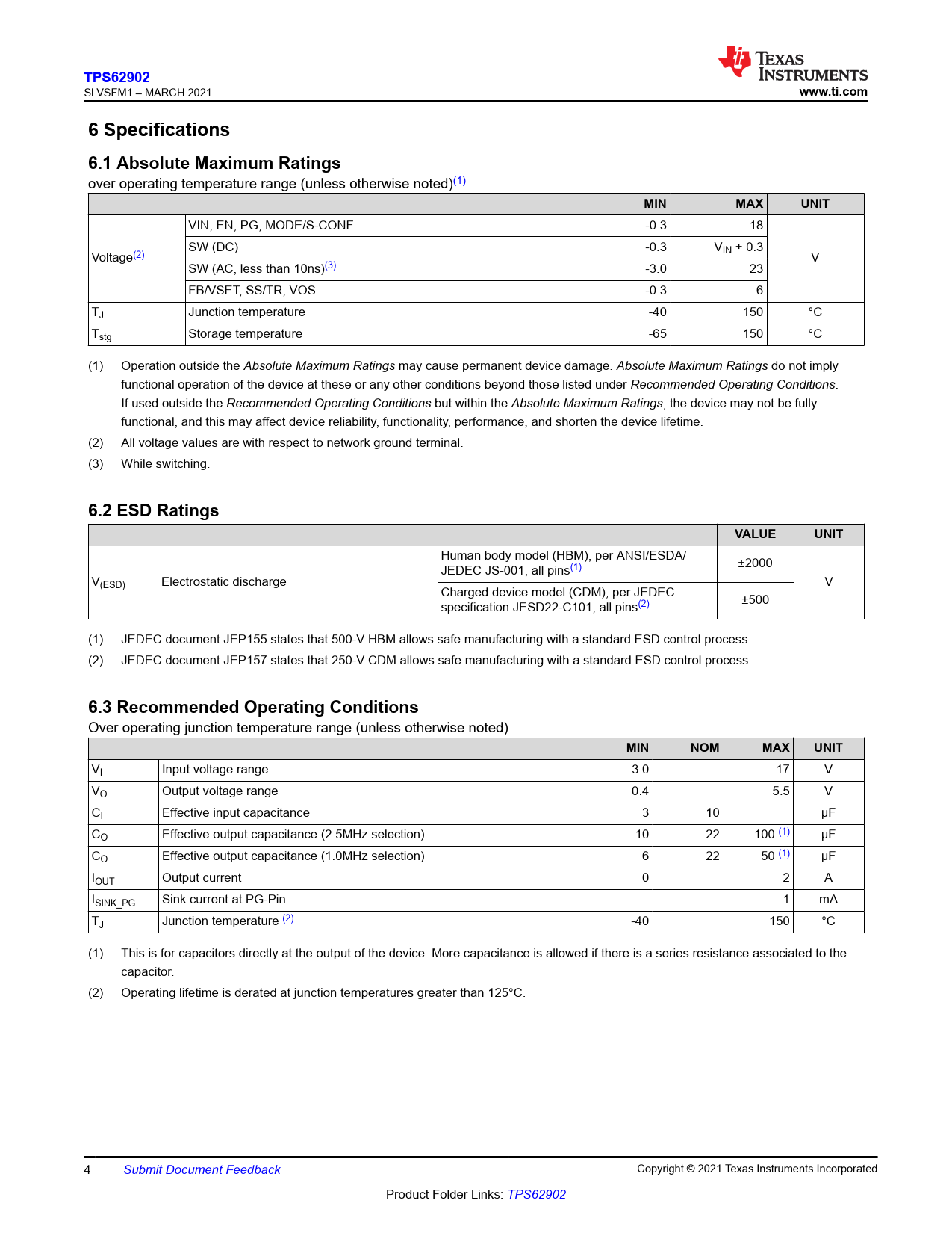
TPS62902. www.ti.com. 6 Specifications. 6.1 Absolute Maximum Ratings. MIN. MAX. UNIT. 6.2 ESD Ratings. VALUE

24 предложений от 9 поставщиков 3-V to 17-V, 2-A, high-efficiency and low IQ buck converter 1.5-mm × 2-mm QFN package |
| TPS62902RPJR
Texas Instruments | 86 ₽ | |
| TPS62902RPJR
| от 139 ₽ | |
| TPS62902RPJR
Texas Instruments | от 155 ₽ | |
| TPS62902RPJR
Texas Instruments | 185 ₽ | |
Модельный ряд для этого даташита
Текстовая версия документа
link to page 4 link to page 4 link to page 4 link to page 4 link to page 4 link to page 4 link to page 4 link to page 4
TPS62902
SLVSFM1 – MARCH 2021
www.ti.com 6 Specifications 6.1 Absolute Maximum Ratings
over operating temperature range (unless otherwise noted)(1)
MIN MAX UNIT
VIN, EN, PG, MODE/S-CONF -0.3 18 SW (DC) -0.3 VIN + 0.3 Voltage(2) V SW (AC, less than 10ns)(3) -3.0 23 FB/VSET, SS/TR, VOS -0.3 6 TJ Junction temperature -40 150 °C Tstg Storage temperature -65 150 °C (1) Operation outside the Absolute Maximum Ratings may cause permanent device damage. Absolute Maximum Ratings do not imply functional operation of the device at these or any other conditions beyond those listed under Recommended Operating Conditions. If used outside the Recommended Operating Conditions but within the Absolute Maximum Ratings, the device may not be fully functional, and this may affect device reliability, functionality, performance, and shorten the device lifetime. (2) All voltage values are with respect to network ground terminal. (3) While switching.
6.2 ESD Ratings VALUE UNIT
Human body model (HBM), per ANSI/ESDA/ JEDEC JS-001, all pins(1) ±2000 V(ESD) Electrostatic discharge V Charged device model (CDM), per JEDEC specification JESD22-C101, all pins(2) ±500 (1) JEDEC document JEP155 states that 500-V HBM allows safe manufacturing with a standard ESD control process. (2) JEDEC document JEP157 states that 250-V CDM allows safe manufacturing with a standard ESD control process.
6.3 Recommended Operating Conditions
Over operating junction temperature range (unless otherwise noted)
MIN NOM MAX UNIT
VI Input voltage range 3.0 17 V VO Output voltage range 0.4 5.5 V CI Effective input capacitance 3 10 µF CO Effective output capacitance (2.5MHz selection) 10 22 100 (1) µF CO Effective output capacitance (1.0MHz selection) 6 22 50 (1) µF IOUT Output current 0 2 A ISINK_PG Sink current at PG-Pin 1 mA TJ Junction temperature (2) -40 150 °C (1) This is for capacitors directly at the output of the device. More capacitance is allowed if there is a series resistance associated to the capacitor. (2) Operating lifetime is derated at junction temperatures greater than 125°C. 4 Submit Document Feedback Copyright © 2021 Texas Instruments Incorporated Product Folder Links: TPS62902 Document Outline 1 Features 2 Applications 3 Description Table of Contents 4 Revision History 5 Pin Configuration and Functions 6 Specifications 6.1 Absolute Maximum Ratings 6.2 ESD Ratings 6.3 Recommended Operating Conditions 6.4 Thermal Information 6.5 Electrical Characteristics 6.6 Typical Characteristics 7 Detailed Description 7.1 Overview 7.2 Functional Block Diagram 7.3 Feature Description 7.3.1 Mode Selection and Device Configuration MODE/S-CONF 7.3.2 Adjustable VO Operation (External Voltage Divider) 7.3.3 Setable VO Operation (VSET and Internal Voltage Divider) 7.3.4 Soft Start / Tracking (SS/TR) 7.3.5 Smart Enable with Precise Threshold 7.3.6 Power Good (PG) 7.3.7 Undervoltage Lockout (UVLO) 7.3.8 Current Limit And Short Circuit Protection 7.3.9 Thermal Shutdown 7.4 Device Functional Modes 7.4.1 Pulse Width Modulation (PWM) Operation 7.4.2 AEE (Automatic Efficiency Enhancement) 7.4.3 Power Save Mode Operation (Auto PFM/PWM) 7.4.4 100% Duty-Cycle Operation 7.4.5 Output Discharge Function 7.4.6 Starting into a Pre-Biased Load 8 Application and Implementation 8.1 Application Information 8.2 Typical Application with Adjustable Output Voltage 8.2.1 Design Requirements 8.2.2 Detailed Design Procedure 8.2.2.1 Custom Design With WEBENCH® Tools 8.2.2.2 Programming the Output Voltage 8.2.2.3 External Component Selection 8.2.2.4 Inductor Selection 8.2.2.5 Capacitor Selection 8.2.2.5.1 Output Capacitor 8.2.2.5.2 Input Capacitor 8.2.2.5.3 Soft-Start Capacitor 8.2.2.6 Tracking Function 8.2.2.7 Output Filter and Loop Stability 8.2.3 Application Curves 8.2.4 Typical Application with Setable VO using VSET 8.2.4.1 Design Requirements 8.2.4.2 Detailed Design Procedure 8.2.4.3 Application Curves 8.3 System Examples 8.3.1 LED Power Supply 8.3.2 Powering Multiple Loads 8.3.3 Voltage Tracking 8.3.4 Precise Soft-Start Timing 9 Power Supply Recommendations 10 Layout 10.1 Layout Guidelines 10.2 Layout Example 10.2.1 Thermal Considerations 11 Device and Documentation Support 11.1 Device Support 11.1.1 Development Support 11.1.1.1 Custom Design With WEBENCH® Tools 11.2 Receiving Notification of Documentation Updates 11.3 Support Resources 11.4 Trademarks 11.5 Electrostatic Discharge Caution 11.6 Glossary 12 Mechanical, Packaging, and Orderable Information

 Купить TPS62902RPJR на РадиоЛоцман.Цены — от 86 до 3 268 ₽