Datasheet AD8315 (Analog Devices)
| Производитель | Analog Devices |
| Описание | 50 dB GSM PA Controller |
| Страниц / Страница | 22 / 1 — 50 dB GSM PA Controller. Data Sheet. AD8315. FEATURES. Complete RF … |
| Версия | D |
| Формат / Размер файла | PDF / 450 Кб |
| Язык документа | английский |
50 dB GSM PA Controller. Data Sheet. AD8315. FEATURES. Complete RF detector/controller function

19 предложений от 14 поставщиков Высокочастотная техника и средства высокочастотной идентификации ВЧ контроллеры усилителей мощности |
| AD8315ARMZ-RL
Analog Devices | 716 ₽ | |
| AD8315ARMZ-RL
Analog Devices | от 765 ₽ | |
| AD8315ARMZ-RL
Rochester Electronics | от 1 308 ₽ | |
| AD8315ARMZ-RL
Analog Devices | от 1 793 ₽ | |
Модельный ряд для этого даташита
Текстовая версия документа
50 dB GSM PA Controller Data Sheet AD8315 FEATURES
Its high sensitivity allows control at low signal levels, thus reducing the amount of power that must be coupled to
Complete RF detector/controller function
the detector.
>50 dB range at 0.9 GHz (−49 dBm to +2 dBm, re 50 Ω) Accurate scaling from 0.1 GHz to 2.5 GHz
For convenience, the signal is internally ac-coupled. This
Temperature-stable linear-in-dB response
high-pass coupling, with a corner at approximately 0.016 GHz,
Log slope of 23 mV/dB, intercept at −60 dBm at 0.9 GHz
determines the lowest operating frequency. Therefore, the
True integration function in control loop
source can be dc grounded.
Low power: 20 mW at 2.7 V, 38 mW at 5 V
The AD8315 provides a voltage output, VAPC, that has the
Power-down to 10.8 μW
voltage range and current drive to directly connect to most
APPLICATIONS
handset power amplifiers’ gain control pin. VAPC can swing from 250 mV above ground to within 200 mV below the supply
Single, dual, and triple band mobile handset (GSM, DCS, EDGE)
voltage. Load currents of up to 6 mA can be supported.
Transmitter power control
The setpoint control input is applied to the VSET pin and has
GENERAL DESCRIPTION
an operating range of 0.25 V to 1.4 V. The associated circuit The AD8315 is a complete low cost subsystem for the precise determines the slope and intercept of the linear-in-dB control of RF power amplifiers operating in the frequency range measurement system; these are nominally 23 mV/dB and 0.1 GHz to 2.5 GHz and over a typical dynamic range of 50 dB. −60 dBm for a 50 Ω termination (−73 dBV) at 0.9 GHz. It is intended for use in cellular handsets and other battery- Further simplifying the application of the AD8315, the input operated wireless devices. The log amp technique provides a much resistance of the setpoint interface is over 100 MΩ, and the bias wider measurement range and better accuracy than controllers current is typically 0.5 μA. using diode detectors. In particular, the temperature stability is The AD8315 is available in MSOP and LFCSP packages and excellent over a specified range of −30°C to +85°C. consumes 8.5 mA from a 2.7 V to 5.5 V supply. When powered down, the sleep current is 4 μA.
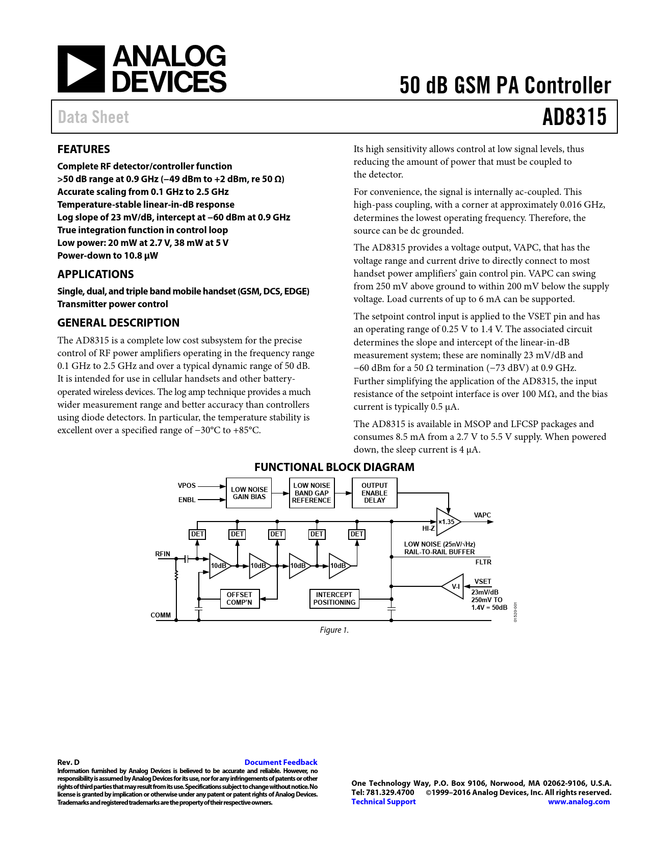
FUNCTIONAL BLOCK DIAGRAM VPOS LOW NOISE OUTPUT LOW NOISE BAND GAP ENABLE ENBL GAIN BIAS REFERENCE DELAY VAPC ×1.35 HI-Z DET DET DET DET DET LOW NOISE (25nV/√Hz) RFIN RAIL-TO-RAIL BUFFER FLTR 10dB 10dB 10dB 10dB VSET V-I OFFSET INTERCEPT 23mV/dB COMP’N POSITIONING 250mV TO 1.4V = 50dB
01 0 0-
COMM
52 01 Figure 1.
Rev. D Document Feedback Information furnished by Analog Devices is believed to be accurate and reliable. However, no responsibility is assumed by Analog Devices for its use, nor for any infringements of patents or other rights of third parties that may result from its use. Specifications subject to change without notice. No One Technology Way, P.O. Box 9106, Norwood, MA 02062-9106, U.S.A. license is granted by implication or otherwise under any patent or patent rights of Analog Devices. Tel: 781.329.4700 ©1999–2016 Analog Devices, Inc. All rights reserved. Trademarks and registered trademarks are the property of their respective owners. Technical Support www.analog.com
Document Outline FEATURES APPLICATIONS GENERAL DESCRIPTION FUNCTIONAL BLOCK DIAGRAM REVISION HISTORY SPECIFICATIONS ABSOLUTE MAXIMUM RATINGS ESD CAUTION PIN CONFIGURATION AND FUNCTION DESCRIPTIONS TYPICAL PERFORMANCE CHARACTERISTICS THEORY OF OPERATION BASIC THEORY CONTROLLER-MODE LOG AMPS CONTROL LOOP DYNAMICS Example PRACTICAL LOOP A NOTE ABOUT POWER EQUIVALENCY BASIC CONNECTIONS RANGE ON VSET AND RFIN TRANSIENT RESPONSE MOBILE HANDSET POWER CONTROL EXAMPLE ENABLE AND POWER-ON INPUT COUPLING OPTIONS USING THE CHIP SCALE PACKAGE EVALUATION BOARD OUTLINE DIMENSIONS ORDERING GUIDE
 Купить AD8315ARMZ-RL на РадиоЛоцман.Цены — от 453 до 41 129 ₽