Datasheet HMC8401 (Analog Devices)
| Производитель | Analog Devices |
| Описание | DC to 28 GHz, GaAs pHEMT MMIC Low Noise Amplifier |
| Страниц / Страница | 17 / 1 — DC to 28 GHz, GaAs, pHEMT,. MMIC, Low Noise Amplifier. Data Sheet. … |
| Версия | B |
| Формат / Размер файла | PDF / 363 Кб |
| Язык документа | английский |
DC to 28 GHz, GaAs, pHEMT,. MMIC, Low Noise Amplifier. Data Sheet. HMC8401. FEATURES. GENERAL DESCRIPTION

16 предложений от 13 поставщиков Высокочастотная техника и средства высокочастотной идентификации ВЧ усилители |
| HMC8401
Analog Devices | от 378 ₽ | |
| HMC8401
Analog Devices | 4 295 ₽ | |
| HMC8401
Analog Devices | 14 318 ₽ | |
| HMC8401
Analog Devices | 24 141 ₽ | |
Модельный ряд для этого даташита
Текстовая версия документа
DC to 28 GHz, GaAs, pHEMT, MMIC, Low Noise Amplifier Data Sheet HMC8401 FEATURES GENERAL DESCRIPTION Output power for 1 dB compression (P1dB): 16.5 dBm typical
The HMC8401 is a gallium arsenide (GaAs), pseudomorphic
Saturated output power (PSAT): 19 dBm typical
high electron mobility transistor (pHEMT), monolithic microwave
Gain: 14.5 dB typical
integrated circuit (MMIC). The HMC8401 is a wideband low
Noise figure: 1.5 dB
noise amplifier which operates between dc and 28 GHz. The
Output third order intercept (IP3): 26 dBm typical
amplifier provides 14.5 dB of gain, 1.5 dB noise figure, 26 dBm
Supply voltage: 7.5 V at 60 mA
output IP3 and 16.5 dBm of output power at 1 dB gain compression
50 Ω matched input/output
while requiring 60 mA from a 7.5 V supply. The HMC8401 also
Die size: 2.55 mm x 1.62 mm x 0.05 mm
has a gain control option, VGG2. The HMC8401 amplifier input/
APPLICATIONS
outputs are internally matched to 50 Ω facilitating integration into multichip modules (MCMs). All data is taken with the chip
Test instrumentation
connected via two 0.025 mm (1 mil) wire bonds of minimal
Microwave radios and very small aperture terminals (VSATs)
length 0.31 mm (12 mils).
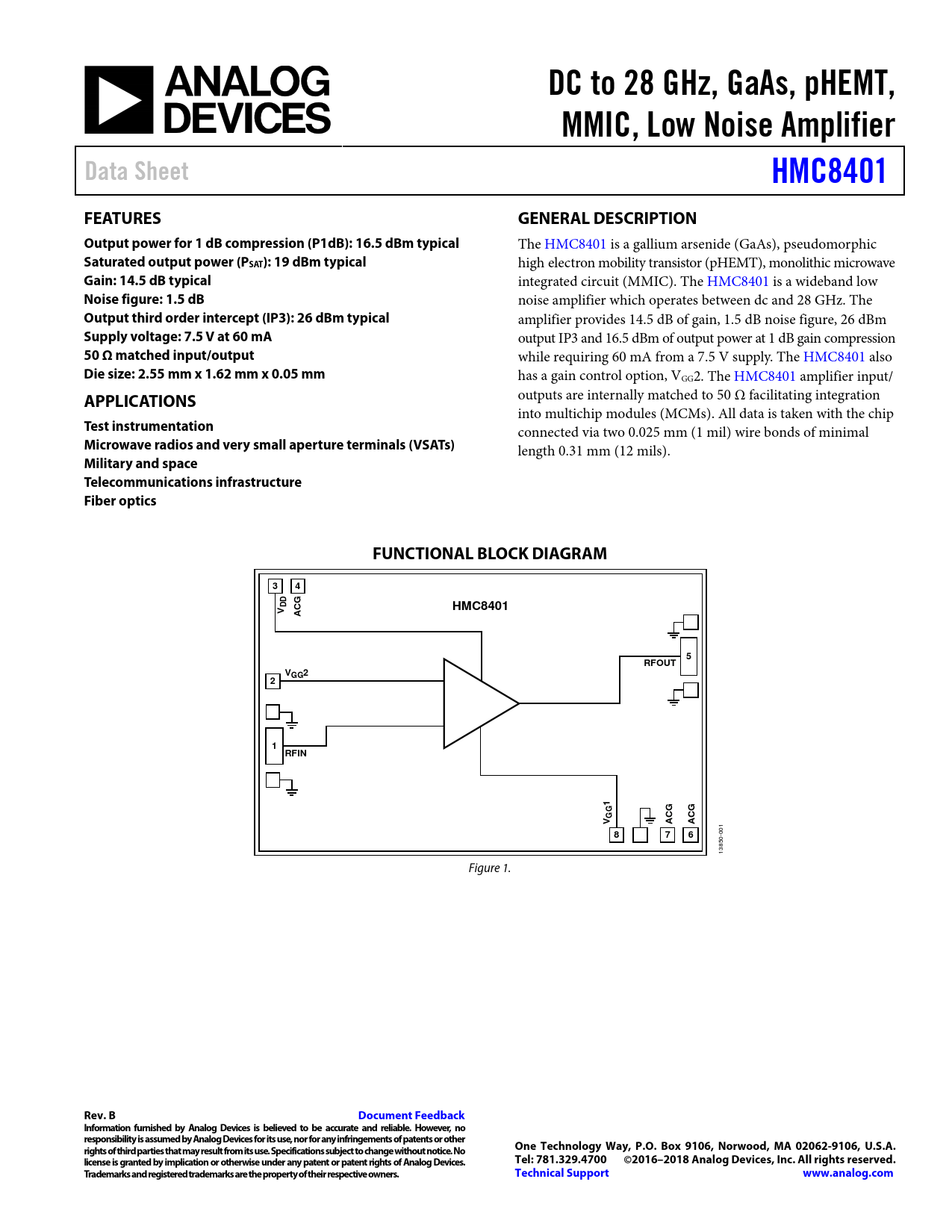
Military and space Telecommunications infrastructure Fiber optics FUNCTIONAL BLOCK DIAGRAM 3 4 DD HMC8401 V ACG 5 RFOUT VGG2 2 1 RFIN 1 GGV ACG ACG 8 7 6
001 13850- Figure 1.
Rev. B Document Feedback Information furnished by Analog Devices is believed to be accurate and reliable. However, no responsibility is assumed by Analog Devices for its use, nor for any infringements of patents or other rights of third parties that may result from its use. Specifications subject to change without notice. No One Technology Way, P.O. Box 9106, Norwood, MA 02062-9106, U.S.A. license is granted by implication or otherwise under any patent or patent rights of Analog Devices. Tel: 781.329.4700 ©2016–2018 Analog Devices, Inc. All rights reserved. Trademarks and registered trademarks are the property of their respective owners. Technical Support www.analog.com
Document Outline Features Applications General Description Functional Block Diagram Table of Contents Revision History Specifications 0.01 GHz to 3 GHz Frequency Range 3 GHz to 26 GHz Frequency Range 26 GHz to 28 GHz Frequency Range Absolute Maximum Ratings ESD Caution Pin Configuration and Function Descriptions Interface Schematics Typical Performance Characteristics Theory of Operation Applications Information Biasing Procedures Mounting and Bonding Techniques for Millimeterwave GaAs MMICs Handling Precautions Mounting Eutectic Die Attach Epoxy Die Attach Wire Bonding Typical Application Circuit Assembly Diagram Outline Dimensions Ordering Guide
 Купить HMC8401 на РадиоЛоцман.Цены — от 378 до 40 854 ₽