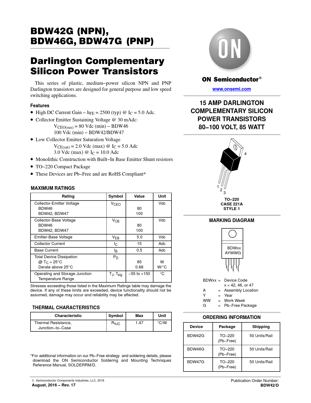
Datasheet BDW42G (NPN), BDW46G, BDW47G (PNP) (ON Semiconductor)
| Производитель | ON Semiconductor |
| Описание | Darlington Complementary Silicon Power Transistors |
| Страниц / Страница | 8 / 1 — www.onsemi.com. 15 AMP DARLINGTON. Features. COMPLEMENTARY SILICON. POWER … |
| Версия | 17 |
| Формат / Размер файла | PDF / 239 Кб |
| Язык документа | английский |
www.onsemi.com. 15 AMP DARLINGTON. Features. COMPLEMENTARY SILICON. POWER TRANSISTORS. 80−100 VOLT, 85 WATT. MAXIMUM RATINGS. Rating

25 предложений от 17 поставщиков Биполярный транзистор, дарлингтона, PNP, 100 В, 15 А, 85 Вт, TO-220, Through Hole |
| BDW47G
ON Semiconductor | 8.78 ₽ | |
| BDW47
ON Semiconductor | 32 ₽ | |
| BDW47G
ON Semiconductor | от 153 ₽ | |
| BDW47G
ON Semiconductor | по запросу | |
Модельный ряд для этого даташита
Текстовая версия документа
BDW42G (NPN), BDW46G,BDW47G (PNP) Darlington Complementary Silicon Power Transistors This series of plastic, medium−power silicon NPN and PNP Darlington transistors are designed for general purpose and low speed
www.onsemi.com
switching applications.
15 AMP DARLINGTON Features
• High DC Current Gain − h
COMPLEMENTARY SILICON
FE = 2500 (typ) @ IC = 5.0 Adc. • Collector Emitter Sustaining Voltage @ 30 mAdc:
POWER TRANSISTORS
VCEO(sus) = 80 Vdc (min) − BDW46
80−100 VOLT, 85 WATT
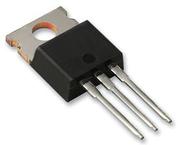
100 Vdc (min) − BDW42/BDW47 • Low Collector Emitter Saturation Voltage VCE(sat) = 2.0 Vdc (max) @ IC = 5.0 Adc 3.0 Vdc (max) @ IC = 10.0 Adc 4 • Monolithic Construction with Built−In Base Emitter Shunt resistors • TO−220 Compact Package • These Devices are Pb−Free and are RoHS Compliant*
MAXIMUM RATINGS
1 2 3
Rating Symbol Value Unit TO−220
Collector-Emitter Voltage VCEO Vdc
CASE 221A
BDW46 80
STYLE 1
BDW42, BDW47 100 Collector-Base Voltage VCB Vdc
MARKING DIAGRAM
BDW46 80 BDW42, BDW47 100 Emitter-Base Voltage VEB 5.0 Vdc Collector Current IC 15 Adc BDWxx Base Current IB 0.5 Adc AYWWG Total Device Dissipation PD @ TC = 25°C 85 W Derate above 25°C 0.68 W/°C Operating and Storage Junction TJ, Tstg −55 to +150 °C Temperature Range BDWxx = Device Code Stresses exceeding those listed in the Maximum Ratings table may damage the x = 42, 46, or 47 device. If any of these limits are exceeded, device functionality should not be A = Assembly Location assumed, damage may occur and reliability may be affected. Y = Year WW = Work Week G = Pb−Free Package
THERMAL CHARACTERISTICS Characteristic Symbol Max Unit ORDERING INFORMATION
Thermal Resistance, RqJC 1.47 °C/W Junction−to−Case
Device Package Shipping
BDW42G TO−220 50 Units/Rail (Pb−Free) BDW46G TO−220 50 Units/Rail *For additional information on our Pb−Free strategy and soldering details, please (Pb−Free) download the ON Semiconductor Soldering and Mounting Techniques BDW47G TO−220 50 Units/Rail Reference Manual, SOLDERRM/D. (Pb−Free) © Semiconductor Components Industries, LLC, 2016 Publication Order Number:
August, 2016 − Rev. 17 BDW42/D

 Купить BDW47 на РадиоЛоцман.Цены — от 8.78 до 153 ₽