Datasheet BV2HD070EFU-C (Rohm) - 10
| Производитель | Rohm |
| Описание | Automotive 2ch 70 mΩ High-Side Switch with Variable OCD and OCD Mask Function |
| Страниц / Страница | 37 / 10 — BV2HD070EFU-C |
| Формат / Размер файла | PDF / 2.9 Мб |
| Язык документа | английский |
BV2HD070EFU-C

Модельный ряд для этого даташита
Текстовая версия документа
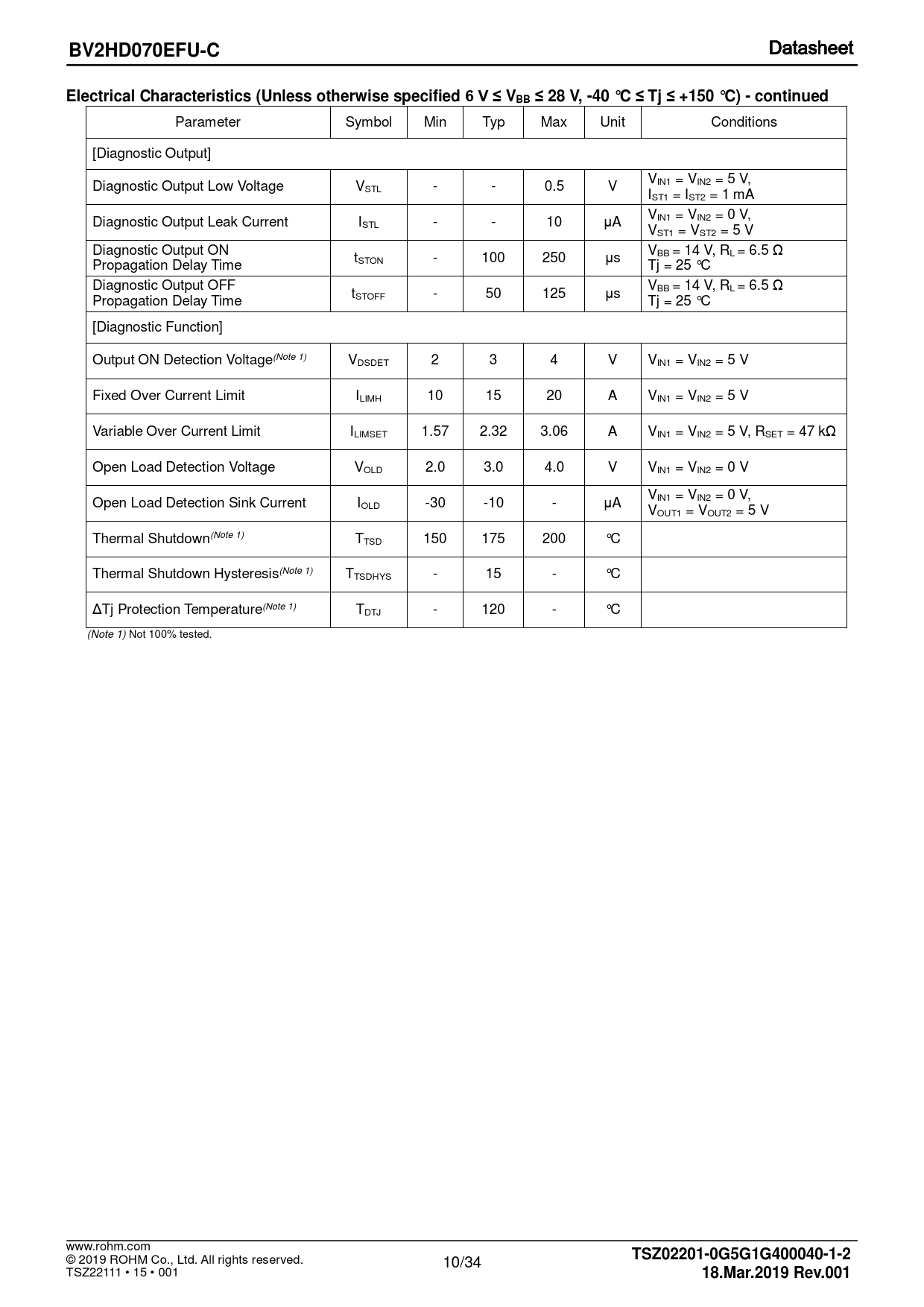
BV2HD070EFU-C Electrical Characteristics (Unless otherwise specified 6 V ≤ VBB ≤ 28 V, -40 °C ≤ Tj ≤ +150 °C) - continued
Parameter Symbol Min Typ Max Unit Conditions [Diagnostic Output] V Diagnostic Output Low Voltage V IN1 = VIN2 = 5 V, STL - - 0.5 V IST1 = IST2 = 1 mA V Diagnostic Output Leak Current I IN1 = VIN2 = 0 V, STL - - 10 μA VST1 = VST2 = 5 V Diagnostic Output ON V t BB = 14 V, RL = 6.5 Ω Propagation Delay Time STON - 100 250 μs Tj = 25 °C Diagnostic Output OFF V t BB = 14 V, RL = 6.5 Ω Propagation Delay Time STOFF - 50 125 μs Tj = 25 °C [Diagnostic Function] Output ON Detection Voltage(Note 1) VDSDET 2 3 4 V VIN1 = VIN2 = 5 V Fixed Over Current Limit ILIMH 10 15 20 A VIN1 = VIN2 = 5 V Variable Over Current Limit ILIMSET 1.57 2.32 3.06 A VIN1 = VIN2 = 5 V, RSET = 47 kΩ Open Load Detection Voltage VOLD 2.0 3.0 4.0 V VIN1 = VIN2 = 0 V V Open Load Detection Sink Current I IN1 = VIN2 = 0 V, OLD -30 -10 - μA VOUT1 = VOUT2 = 5 V Thermal Shutdown(Note 1) TTSD 150 175 200 °C Thermal Shutdown Hysteresis(Note 1) TTSDHYS - 15 - °C ΔTj Protection Temperature(Note 1) TDTJ - 120 - °C (Note 1) Not 100% tested. www.rohm.com
TSZ02201-0G5G1G400040-1-2
© 2019 ROHM Co., Ltd. All rights reserved. 10/34 TSZ22111 • 15 • 001
18.Mar.2019 Rev.001
Document Outline General Description Features Applications Key Specifications Package Typical Application Circuit Table of Contents Pin Configuration Pin Description Block Diagram Definition Absolute Maximum Ratings Thermal Resistance Recommended Operating Conditions Electrical Characteristics Typical Performance Curves Figure 6. Standby Current vs Supply Voltage Figure 7. Standby Current vs Junction Temperature Figure 8. Operating Current vs Supply Voltage Figure 9. Operating Current vs Junction Temperature Figure 10. UVLO Detection Voltage vs Junction Temperature Figure 11. Input Voltage vs Junction Temperature Figure 12. Input Current vs Junction Temperature Figure 13. Output ON Resistance vs Supply Voltage Figure 14. Output ON Resistance vs Junction Temperature Figure 15. Output leak Current vs Junction Temperature Figure 16. Output Slew Rate vs Junction Temperature Figure 17. Output ON, OFF Propagation Delay Time vs Junction Temperature Figure 18. Output Clamp Voltage vs Junction Temperature Figure 19. Diagnostic Output Low Voltage vs Junction Temperature Figure 20. Diagnostic Output ON, OFF Propagation Delay Time vs Junction Temperature Figure 21. Variable Over Current Limit vs Junction Temperature Figure 22. Open Load Detection Voltage vs Junction Temperature Figure 23. Active Clamp Energy vs Output Current Measurement Circuit Timing Chart (Propagation Delay Time) Function Description 1. Protection Function 2. Over Current Protection 2.1 Over Current Limiting Operation in one side channel 2.2 Over Current Detection in Both Outputs 2.3 Over Current Detection by Other Channel while CDLY is Charging (tDLY) 2.4 Setting of Variable Overcurrent Limit Value 2.5 Variable Over Current Limit Mask Time Setting 2.6 The SET Pin and the DLY Pin Setting 3. Open Load Detection 3.1 When the OUT1, OUT2 is pulled down by the load (Normal function) 3.2 If the SW1 is OFF, the output is no longer pulled down by the load 4. Thermal Shutdown, ΔTj Protection Detection 4.1 Thermal Shutdown Protection 4.2 ΔTj Protection 5. Other Protection 5.1 GND Open Protection 5.2 MCU I/O Protection Applications Example I/O Equivalence Circuits Operational Notes 1. Reverse Connection of Power Supply 2. Power Supply Lines 3. Ground Voltage 4. Ground Wiring Pattern 5. Recommended Operating Conditions 6. Inrush Current 7. Testing on Application Boards 8. Inter-pin Short and Mounting Errors 9. Unused Input Pins 10. Ceramic Capacitor 11. Thermal Shutdown Function (TSD) 12. Over Current Protection Function (OCP) 13. Active Clamp Operation 14. Open Power Supply Pin 15. Open GND Pin Ordering Information Marking Diagram Physical Dimension and Packing Information Revision History
 Купить BV2HD070EFU-CE2 на РадиоЛоцман.Цены — от 44 до 413 ₽