Datasheet LTC3859AL (Analog Devices) - 4
| Производитель | Analog Devices |
| Описание | Triple Output, Buck/Buck/Boost Synchronous Controller with 28μA Burst Mode IQ |
| Страниц / Страница | 44 / 4 — ELECTRICAL. CHARACTERISTICS The. denotes the specifications which apply … |
| Версия | B |
| Формат / Размер файла | PDF / 1.2 Мб |
| Язык документа | английский |
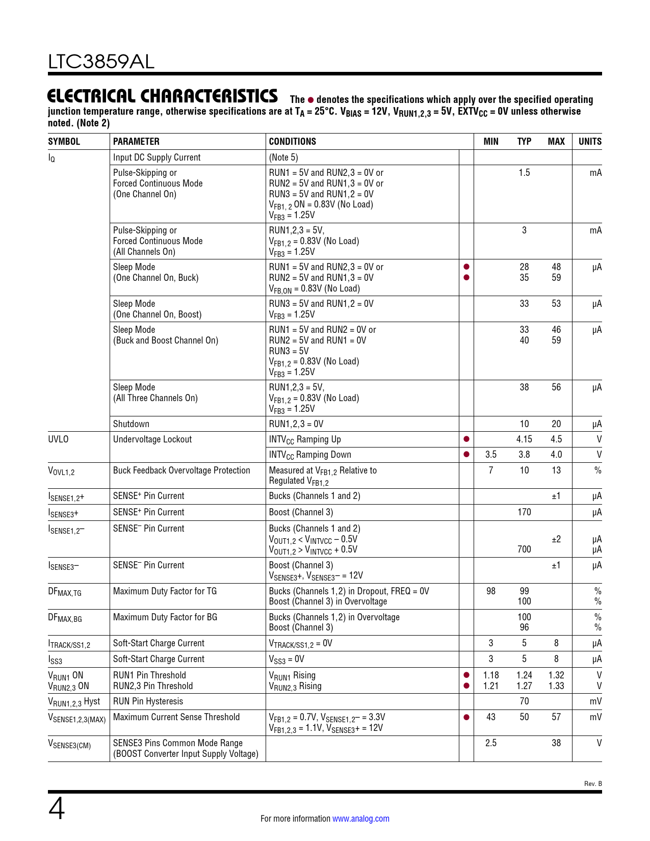
ELECTRICAL. CHARACTERISTICS The. denotes the specifications which apply over the specified operating

Модельный ряд для этого даташита
Текстовая версия документа
LTC3859AL
ELECTRICAL CHARACTERISTICS The
l
denotes the specifications which apply over the specified operating junction temperature range, otherwise specifications are at TA = 25°C. VBIAS = 12V, VRUN1,2,3 = 5V, EXTVCC = 0V unless otherwise noted. (Note 2) SYMBOL PARAMETER CONDITIONS MIN TYP MAX UNITS
IQ Input DC Supply Current (Note 5) Pulse-Skipping or RUN1 = 5V and RUN2,3 = 0V or 1.5 mA Forced Continuous Mode RUN2 = 5V and RUN1,3 = 0V or (One Channel On) RUN3 = 5V and RUN1,2 = 0V VFB1, 2 ON = 0.83V (No Load) VFB3 = 1.25V Pulse-Skipping or RUN1,2,3 = 5V, 3 mA Forced Continuous Mode VFB1,2 = 0.83V (No Load) (All Channels On) VFB3 = 1.25V Sleep Mode RUN1 = 5V and RUN2,3 = 0V or l 28 48 µA (One Channel On, Buck) RUN2 = 5V and RUN1,3 = 0V l 35 59 VFB,ON = 0.83V (No Load) Sleep Mode RUN3 = 5V and RUN1,2 = 0V 33 53 µA (One Channel On, Boost) VFB3 = 1.25V Sleep Mode RUN1 = 5V and RUN2 = 0V or 33 46 µA (Buck and Boost Channel On) RUN2 = 5V and RUN1 = 0V 40 59 RUN3 = 5V VFB1,2 = 0.83V (No Load) VFB3 = 1.25V Sleep Mode RUN1,2,3 = 5V, 38 56 µA (All Three Channels On) VFB1,2 = 0.83V (No Load) VFB3 = 1.25V Shutdown RUN1,2,3 = 0V 10 20 µA UVLO Undervoltage Lockout INTVCC Ramping Up l 4.15 4.5 V INTVCC Ramping Down l 3.5 3.8 4.0 V VOVL1,2 Buck Feedback Overvoltage Protection Measured at VFB1,2 Relative to 7 10 13 % Regulated VFB1,2 ISENSE1,2+ SENSE+ Pin Current Bucks (Channels 1 and 2) ±1 µA ISENSE3+ SENSE+ Pin Current Boost (Channel 3) 170 µA ISENSE1,2– SENSE– Pin Current Bucks (Channels 1 and 2) VOUT1,2 < VINTVCC – 0.5V ±2 µA VOUT1,2 > VINTVCC + 0.5V 700 µA ISENSE3– SENSE– Pin Current Boost (Channel 3) ±1 µA VSENSE3+, VSENSE3– = 12V DFMAX,TG Maximum Duty Factor for TG Bucks (Channels 1,2) in Dropout, FREQ = 0V 98 99 % Boost (Channel 3) in Overvoltage 100 % DFMAX,BG Maximum Duty Factor for BG Bucks (Channels 1,2) in Overvoltage 100 % Boost (Channel 3) 96 % ITRACK/SS1,2 Soft-Start Charge Current VTRACK/SS1,2 = 0V 3 5 8 µA ISS3 Soft-Start Charge Current VSS3 = 0V 3 5 8 µA VRUN1 ON RUN1 Pin Threshold VRUN1 Rising l 1.18 1.24 1.32 V VRUN2,3 ON RUN2,3 Pin Threshold VRUN2,3 Rising l 1.21 1.27 1.33 V VRUN1,2,3 Hyst RUN Pin Hysteresis 70 mV VSENSE1,2,3(MAX) Maximum Current Sense Threshold VFB1,2 = 0.7V, VSENSE1,2– = 3.3V l 43 50 57 mV VFB1,2,3 = 1.1V, VSENSE3+ = 12V VSENSE3(CM) SENSE3 Pins Common Mode Range 2.5 38 V (BOOST Converter Input Supply Voltage) Rev. B 4 For more information www.analog.com Document Outline Features Applications Typical Application Description Absolute Maximum Ratings Pin Configuration Order Information Electrical Characteristics Typical Performance Characteristics Pin Functions Functional Diagram Operation Applications Information Typical Applications Package Description Revision History Typical Application Related Parts

 Купить LTC3859ALMPUHF#PBF на РадиоЛоцман.Цены — от 710 до 3 926 ₽