Datasheet AD8651, AD8652 (Analog Devices)
| Производитель | Analog Devices |
| Описание | 50 MHz, Precision Low Distortion, Low Noise CMOS Dual Op Amp |
| Страниц / Страница | 20 / 1 — 50 MHz, Precision, Low Distortion,. Low Noise CMOS Amplifiers. Data … |
| Версия | D |
| Формат / Размер файла | PDF / 468 Кб |
| Язык документа | английский |
50 MHz, Precision, Low Distortion,. Low Noise CMOS Amplifiers. Data Sheet. AD8651/. AD8652. FEATURES. PIN CONFIGURATIONS

30 предложений от 17 поставщиков Интегральные микросхемы Аналоговая техника — усилители — инструменты, ОУ (операционные), буферные |
| AD8651ARMZ-R2
Analog Devices | 80 ₽ | |
| AD8651ARMZ-REEL
Analog Devices | 118 ₽ | |
| AD8651ARMZ-REEL
Analog Devices | 124 ₽ | |
| AD8651ARMZ-REEL
Analog Devices | по запросу | |
Модельный ряд для этого даташита
Текстовая версия документа
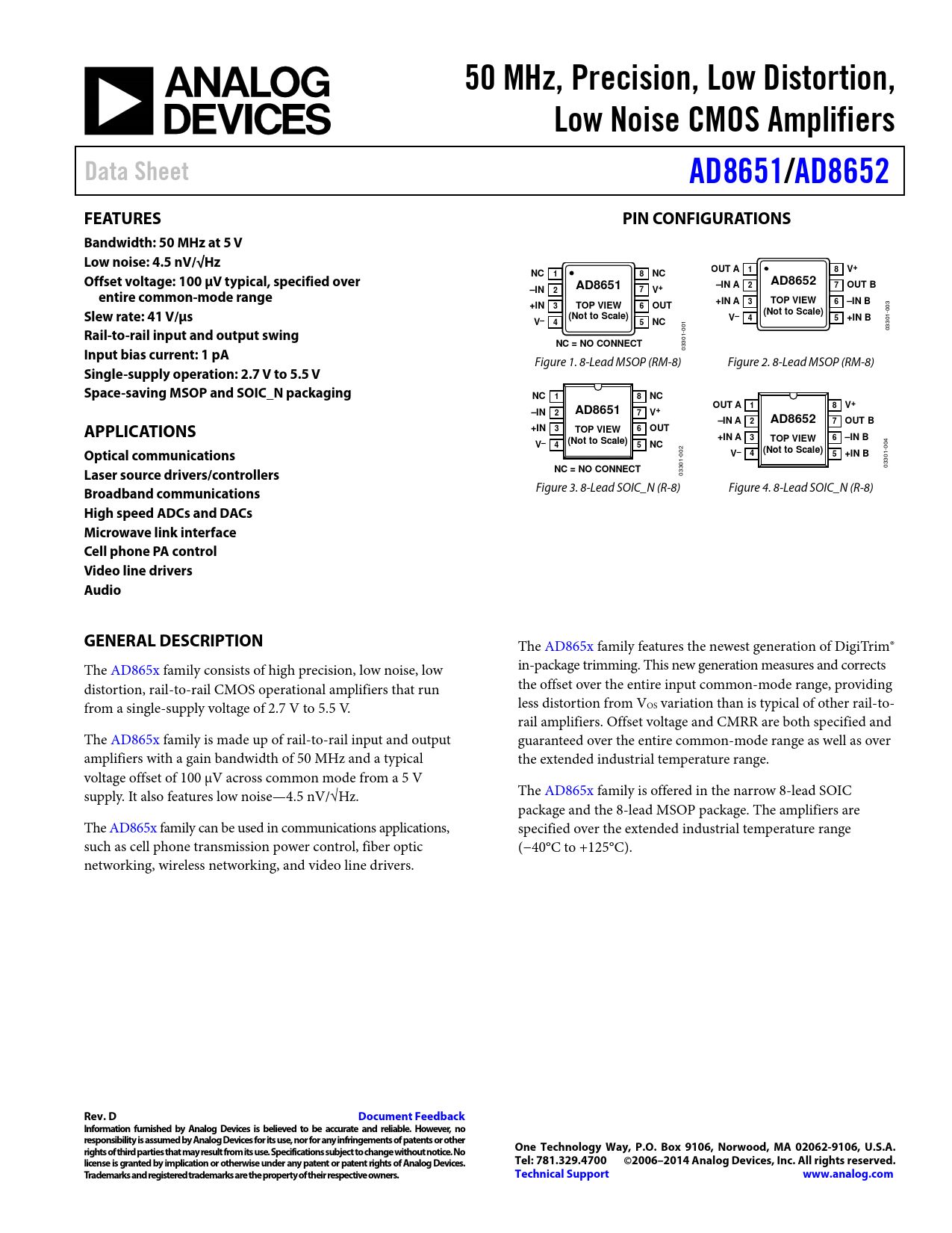
50 MHz, Precision, Low Distortion, Low Noise CMOS Amplifiers Data Sheet AD8651/ AD8652 FEATURES PIN CONFIGURATIONS Bandwidth: 50 MHz at 5 V Low noise: 4.5 nV/√Hz OUT A 8 V+ NC 1 1 8 NC Offset voltage: 100 μV typical, specified over –IN A AD8652 7 OUT B –IN AD8651 2 2 V+ 7 entire common-mode range +IN A TOP VIEW 6 –IN B +IN 3 3 TOP VIEW 6 OUT
03 0
Slew rate: 41 V/μs (Not to Scale) (Not to Scale) V– 5 +IN B
1-
V– 4 4 5 NC
1 30 00 03
Rail-to-rail input and output swing
1-
NC = NO CONNECT
30 03
Input bias current: 1 pA
Figure 1. 8-Lead MSOP (RM-8) Figure 2. 8-Lead MSOP (RM-8)
Single-supply operation: 2.7 V to 5.5 V Space-saving MSOP and SOIC_N packaging NC 1 8 NC OUT A 1 V+ 8 –IN 2 AD8651 V+ 7 –IN A 2 AD8652 7 OUT B APPLICATIONS +IN 3 TOP VIEW 6 OUT +IN A 3 TOP VIEW 6 –IN B
4
V– (Not to Scale) 4 5 NC
-00
Optical communications
02
(Not to Scale)
0
V– 4 5 +IN B
1- 301 03
Laser source drivers/controllers NC = NO CONNECT
330 0
Broadband communications
Figure 3. 8-Lead SOIC_N (R-8) Figure 4. 8-Lead SOIC_N (R-8)
High speed ADCs and DACs Microwave link interface Cell phone PA control Video line drivers Audio GENERAL DESCRIPTION
The AD865x family features the newest generation of DigiTrim® The AD865x family consists of high precision, low noise, low in-package trimming. This new generation measures and corrects distortion, rail-to-rail CMOS operational amplifiers that run the offset over the entire input common-mode range, providing from a single-supply voltage of 2.7 V to 5.5 V. less distortion from VOS variation than is typical of other rail-to- rail amplifiers. Offset voltage and CMRR are both specified and The AD865x family is made up of rail-to-rail input and output guaranteed over the entire common-mode range as well as over amplifiers with a gain bandwidth of 50 MHz and a typical the extended industrial temperature range. voltage offset of 100 μV across common mode from a 5 V supply. It also features low noise—4.5 nV/√Hz. The AD865x family is offered in the narrow 8-lead SOIC package and the 8-lead MSOP package. The amplifiers are The AD865x family can be used in communications applications, specified over the extended industrial temperature range such as cell phone transmission power control, fiber optic (−40°C to +125°C). networking, wireless networking, and video line drivers.
Rev. D Document Feedback Information furnished by Analog Devices is believed to be accurate and reliable. However, no responsibility is assumed by Analog Devices for its use, nor for any infringements of patents or other rights of third parties that may result from its use. Specifications subject to change without notice. No One Technology Way, P.O. Box 9106, Norwood, MA 02062-9106, U.S.A. license is granted by implication or otherwise under any patent or patent rights of Analog Devices. Tel: 781.329.4700 ©2006–2014 Analog Devices, Inc. All rights reserved. Trademarks and registered trademarks are the property of their respective owners. Technical Support www.analog.com
Document Outline Features Applications Pin Configurations General Description Table of Contents Revision History Specifications Electrical Characteristics Absolute Maximum Ratings ESD Caution Thermal Resistance Typical Performance Characteristics Applications Theory of Operation Rail-to-Rail Output Stage Rail-to-Rail Input Stage Input Protection Overdrive Recovery Layout, Grounding, and Bypassing Considerations Power Supply Bypassing Grounding Leakage Currents Input Capacitance Output Capacitance Settling Time THD Readings vs. Common-Mode Voltage Driving a 16-Bit ADC Outline Dimensions Ordering Guide

 Купить AD8651ARMZ на РадиоЛоцман.Цены — от 80 до 563 ₽