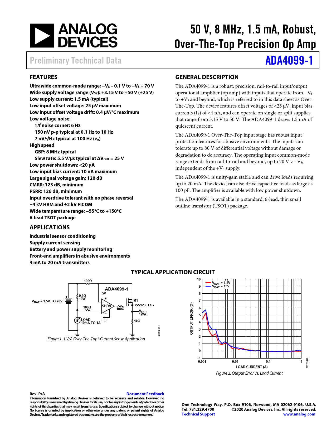
Datasheet ADA4099-1 (Analog Devices)
| Производитель | Analog Devices |
| Описание | 50 V, 8 MHz, 1.5 mA, Robust, Over-The-Top Precision Op Amp |
| Страниц / Страница | 26 / 1 — 50 V, 8 MHz, 1.5 mA, Robust,. Over-The-Top Precision Op Amp. Preliminary … |
| Версия | PrA |
| Формат / Размер файла | PDF / 577 Кб |
| Язык документа | английский |
50 V, 8 MHz, 1.5 mA, Robust,. Over-The-Top Precision Op Amp. Preliminary Technical Data. ADA4099-1. FEATURES. GENERAL DESCRIPTION

Модельный ряд для этого даташита
Текстовая версия документа
50 V, 8 MHz, 1.5 mA, Robust, Over-The-Top Precision Op Amp Preliminary Technical Data ADA4099-1 FEATURES GENERAL DESCRIPTION Ultrawide common-mode range: −VS – 0.1 V to −VS + 70 V
The ADA4099-1 is a robust, precision, rail-to-rail input/output
Wide supply voltage range (VSY): +3.15 V to +50 V (±25 V)
operational amplifier (op amp) with inputs that operate from −VS
Low supply current: 1.5 mA (typical)
to +VS and beyond, which is referred to in this data sheet as Over-
Low input offset voltage: 25 μV maximum
The-Top. The device features offset voltages of <25 μV, input bias
Low input offset voltage drift: 0.4 μV/°C maximum
currents (IB) of <4 nA, and can operate on single or split supplies
Low voltage noise:
that range from 3.15 V to 50 V. The ADA4099-1 draws 1.5 mA of
1/f noise corner: 6 Hz
quiescent current.
150 nV p-p typical at 0.1 Hz to 10 Hz
The ADA4099-1 Over-The-Top input stage has robust input
7 nV/√Hz typical at 100 Hz (en)
protection features for abusive environments. The inputs can
High speed
tolerate up to 80 V of differential voltage without damage or
GBP: 8 MHz typical
degradation to dc accuracy. The operating input common-mode
Slew rate: 5.5 V/μs typical at ΔVOUT = 25 V
range extends from rail-to-rail and beyond, up to 70 V > –VS,
Low power shutdown: <20 μA
independent of the +VS supply.
Low input bias current: 10 nA maximum Large signal voltage gain: 120 dB
The ADA4099-1 is unity-gain stable and can drive loads requiring
CMRR: 123 dB, minimum
up to 20 mA. The device can also drive capacitive loads as large as
PSRR: 126 dB, minimum
100 pF. The amplifier is available with low power shutdown.
Input overdrive tolerant with no phase reversal
The ADA4099-1 is available in a standard, 6-lead, thin small
±4 kV HBM and ±2 kV FICDM
outline transistor (TSOT) package.
Wide temperature range: −55°C to +150°C 6-lead TSOT package APPLICATIONS Industrial sensor conditioning Supply current sensing Battery and power supply monitoring Front-end amplifiers in abusive environments 4 mA to 20 mA transmitters TYPICAL APPLICATION CIRCUIT 100Ω 10 VBAT = 1.5V 9 V ADA4099-1 BAT = 15V 5V 8 0.1Ω 10W V M1 BAT = 1.5V TO 70V 7 ) BSS123LT1G 100Ω SHDN (% 100Ω 6 V R OUT 1V/A 5 RRO LOAD 1kΩ E 10mA TO 1A 4 UT P
001
3 UT
172-
O
22
2
Figure 1. 1 V/A Over-The-Top® Current Sense Application
1 0 –1 0.001 0.01 0.1 1
002 2-
LOAD CURRENT (A)
2217 Figure 2. Output Error vs. Load Current
Rev. PrA Document Feedback Information furnished by Analog Devices is believed to be accurate and reliable. However, no responsibility is assumed by Analog Devices for its use, nor for any infringements of patents or other rights of third parties that may result from its use. Specifications subject to change without notice. One Technology Way, P.O. Box 9106, Norwood, MA 02062-9106, U.S.A. No license is granted by implication or otherwise under any patent or patent rights of Analog Tel: 781.329.4700 ©2020 Analog Devices, Inc. All rights reserved. Devices. Trademarks and registered trademarks are the property of their respective owners. Technical Support www.analog.com
Document Outline FEATURES APPLICATIONS GENERAL DESCRIPTION TYPICAL APPLICATION CIRCUIT TABLE OF CONTENTS SPECIFICATIONS 5 V SUPPLY ±15 V SUPPLY ABSOLUTE MAXIMUM RATINGS MAXIMUM POWER DISSIPATION THERMAL RESISTANCE ESD CAUTION PIN CONFIGURATION AND FUNCTION DESCRIPTIONS TYPICAL PERFORMANCE CHARACTERISTICS THEORY OF OPERATION INPUT PROTECTION OVER-THE-TOP OPERATION CONSIDERATIONS OUTPUT SHUTDOWN PIN (SHDN) APPLICATIONS INFORMATION LARGE RESISTOR GAIN OPERATION RECOMMENDED VALUES FOR VARIOUS GAINS NOISE DISTORTION POWER DISSIPATION AND THERMAL SHUTDOWN CIRCUIT LAYOUT CONSIDERATIONS POWER SUPPLY BYPASSING GROUNDING ESD PROTECTION WHEN POWERED RELATED PRODUCTS TYPICAL APPLICATIONS OUTLINE DIMENSIONS

 Купить ADA4099-1HUJZ-RL7 на РадиоЛоцман.Цены — от 123 до 1 092 ₽