Datasheet AL8116 (Diodes) - 4
| Производитель | Diodes |
| Описание | Flexible 0-10V Dimming Signal Interface Controller |
| Страниц / Страница | 13 / 4 — AL8116. Absolute Maximum Ratings. Symbol. Parameter. Rating. Unit. … |
| Формат / Размер файла | PDF / 745 Кб |
| Язык документа | английский |
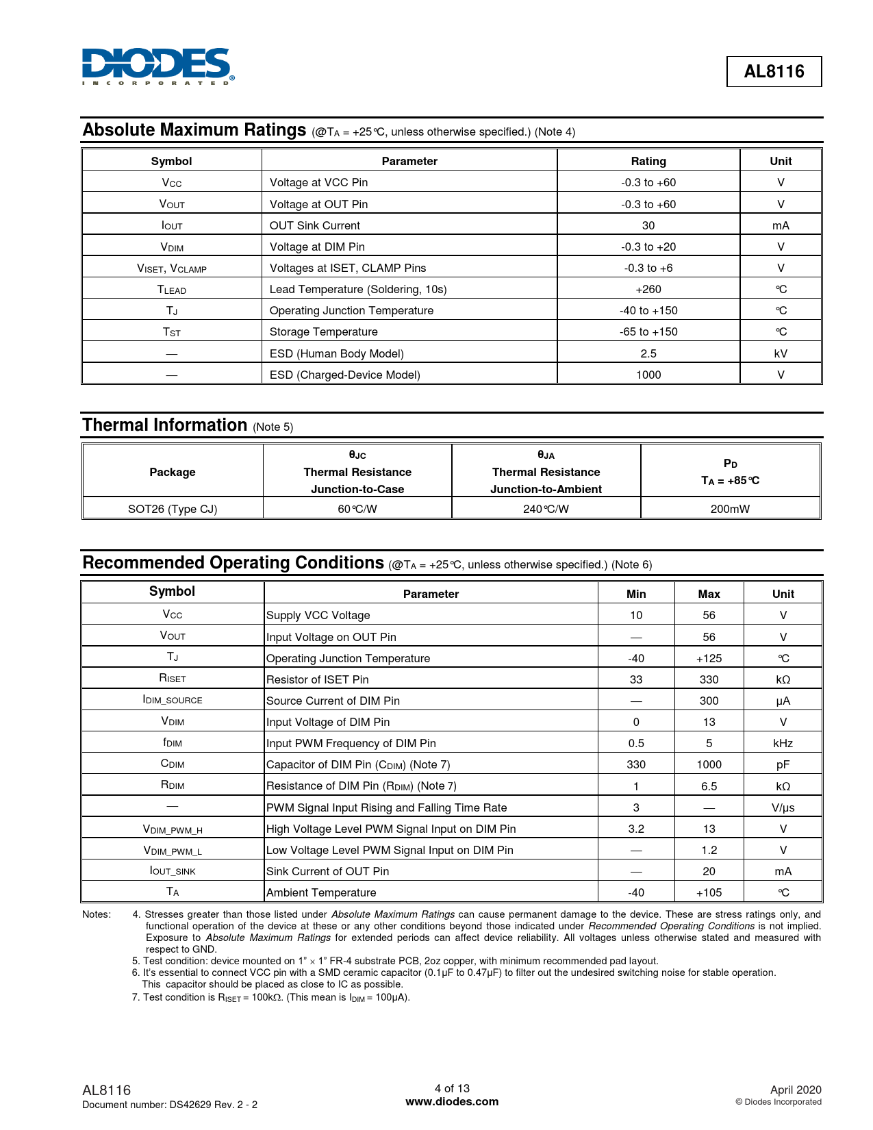
AL8116. Absolute Maximum Ratings. Symbol. Parameter. Rating. Unit. Thermal Information. θJC. θJA. Package. Thermal Resistance. TA = +85°C

Модельный ряд для этого даташита
Текстовая версия документа
AL8116 Absolute Maximum Ratings
(@TA = +25°C, unless otherwise specified.) (Note 4)
Symbol Parameter Rating Unit
VCC Voltage at VCC Pin -0.3 to +60 V VOUT Voltage at OUT Pin -0.3 to +60 V IOUT OUT Sink Current 30 mA VDIM Voltage at DIM Pin -0.3 to +20 V VISET, VCLAMP Voltages at ISET, CLAMP Pins -0.3 to +6 V TLEAD Lead Temperature (Soldering, 10s) +260 °C TJ Operating Junction Temperature -40 to +150 °C TST Storage Temperature -65 to +150 °C — ESD (Human Body Model) 2.5 kV — ESD (Charged-Device Model) 1000 V
Thermal Information
(Note 5)
θJC θJA PD Package Thermal Resistance Thermal Resistance TA = +85°C Junction-to-Case Junction-to-Ambient
SOT26 (Type CJ) 60°C/W 240°C/W 200mW
Recommended Operating Conditions
(@TA = +25°C, unless otherwise specified.) (Note 6)
Symbol Parameter Min Max Unit
VCC Supply VCC Voltage 10 56 V VOUT Input Voltage on OUT Pin — 56 V TJ Operating Junction Temperature -40 +125 °C RISET Resistor of ISET Pin 33 330 kΩ IDIM_SOURCE Source Current of DIM Pin — 300 μA VDIM Input Voltage of DIM Pin 0 13 V fDIM Input PWM Frequency of DIM Pin 0.5 5 kHz CDIM Capacitor of DIM Pin (CDIM) (Note 7) 330 1000 pF RDIM Resistance of DIM Pin (RDIM) (Note 7) 1 6.5 kΩ — PWM Signal Input Rising and Falling Time Rate 3 — V/μs VDIM_PWM_H High Voltage Level PWM Signal Input on DIM Pin 3.2 13 V VDIM_PWM_L Low Voltage Level PWM Signal Input on DIM Pin — 1.2 V IOUT_SINK Sink Current of OUT Pin — 20 mA TA Ambient Temperature -40 +105 °C Notes: 4. Stresses greater than those listed under Absolute Maximum Ratings can cause permanent damage to the device. These are stress ratings only, and functional operation of the device at these or any other conditions beyond those indicated under Recommended Operating Conditions is not implied. Exposure to Absolute Maximum Ratings for extended periods can affect device reliability. All voltages unless otherwise stated and measured with respect to GND. 5. Test condition: device mounted on 1” 1” FR-4 substrate PCB, 2oz copper, with minimum recommended pad layout. 6. It’s essential to connect VCC pin with a SMD ceramic capacitor (0.1μF to 0.47μF) to filter out the undesired switching noise for stable operation. This capacitor should be placed as close to IC as possible. 7. Test condition is RISET = 100k. (This mean is IDIM = 100μA). AL8116 4 of 13 April 2020 Document number: DS42629 Rev. 2 - 2
www.diodes.com
© Diodes Incorporated
 Купить AL8116W6-7 на РадиоЛоцман.Цены — от 6.68 до 2 194 ₽