Datasheet PI4IOE5V9554 (Diodes) - 9
| Производитель | Diodes |
| Описание | 2 8-bit I C-Bus and SMBus I/O Port with Interrupt |
| Страниц / Страница | 17 / 9 — PI4IOE5V9554/9554A. Power-on Reset. c. Interrupt Output. d. I/O Port. … |
| Формат / Размер файла | PDF / 887 Кб |
| Язык документа | английский |
PI4IOE5V9554/9554A. Power-on Reset. c. Interrupt Output. d. I/O Port. www.diodes.com

Модельный ряд для этого даташита
Текстовая версия документа
PI4IOE5V9554/9554A Power-on Reset
When power is applied to VCC, an internal power-on reset (POR) holds thePI4IOE5V9554/PI4IOE5V9554A in a reset condition until VCC has reached VPOR. At that point, the reset condition is released and thePI4IOE5V9554/PI4IOE5V9554A registers and state machine initialize to their default states. Thereafter, VCC must be lowered below 0.2 V to reset the device. For a power reset cycle, VCC must be lowered below 0.2 V and then restored to the operating voltage.
c. Interrupt Output
The open-drain interrupt output is activated when one of the port pins change state and the pin is configured as an input. The interrupt is deactivated when the input returns to its previous state or the input port register is read. Note that changing an I/O from and output to an input may cause a false interrupt to occur if the state of the pin does not match the contents of the input port register.
d. I/O Port
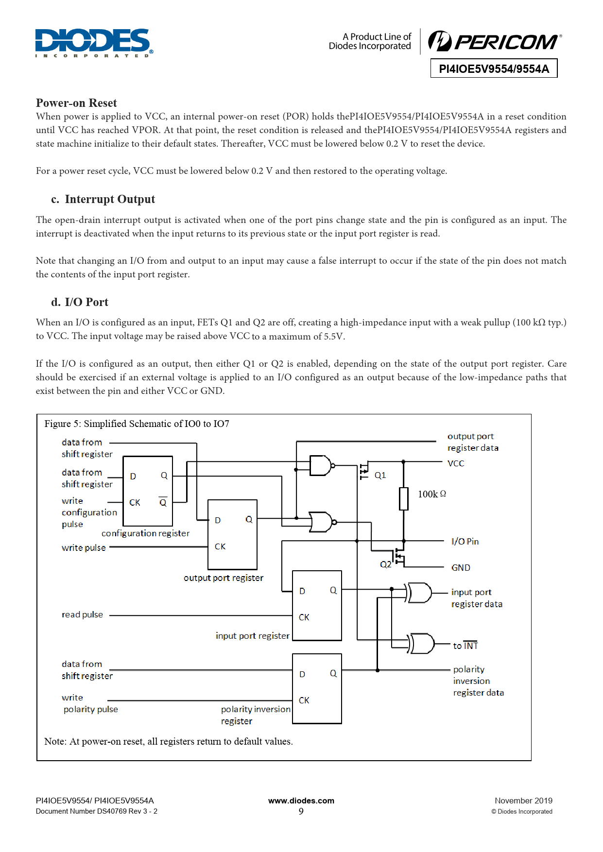
When an I/O is configured as an input, FETs Q1 and Q2 are off, creating a high-impedance input with a weak pullup (100 kΩ typ.) to VCC. The input voltage may be raised above VCC to a maximum of 5.5V. If the I/O is configured as an output, then either Q1 or Q2 is enabled, depending on the state of the output port register. Care should be exercised if an external voltage is applied to an I/O configured as an output because of the low-impedance paths that exist between the pin and either VCC or GND. Figure 5: Simplified Schematic of IO0 to IO7 100kΩ Note: At power-on reset, all registers return to default values. PI4IOE5V9554/ PI4IOE5V9554A
www.diodes.com
November 2019 Document Number DS40769 Rev 3 - 2 9 © Diodes Incorporated Document Outline — Supply Voltage fSCL = 400kHz Supply Current — VI = GND fSCL = 0kHz I/O = inputs Standby Current VI = VCC fSCL = 0kHz I/O = inputs Power-on Reset Voltage[1]

 Купить PI4IOE5V9554LE на РадиоЛоцман.Цены — от 13 до 372 ₽