DatasheetsDatasheet ADuCM3027, ADuCM3029 (Analog …
Datasheet ADuCM3027, ADuCM3029 (Analog Devices)
| Производитель | Analog Devices |
| Описание | Ultra Low Power ARM Cortex-M3 MCU with Integrated Power Management |
| Страниц / Страница | 39 / 1 — Ultra Low Power Arm Cortex-M3 MCU with. Integrated Power Management. Data … |
| Версия | B |
| Формат / Размер файла | PDF / 698 Кб |
| Язык документа | английский |
Ultra Low Power Arm Cortex-M3 MCU with. Integrated Power Management. Data Sheet. ADuCM3027. /ADuCM3029. FEATURES

19 предложений от 10 поставщиков IC MCU 32BIT 256KB FLASH 54WLCSP / ARM? Cortex?-M3 ADuCM Microcontroller IC 32-Bit Single-Core 26MHz 256KB (256K x 8) FLASH 54-WLCSP... |
| ADUCM3029BCBZ-R7
Analog Devices | от 464 ₽ | |
| ADUCM3029BCBZ-R7
Analog Devices | от 497 ₽ | |
| ADUCM3029BCBZ-R7
Analog Devices | 1 463 ₽ | |
| ADUCM3029BCBZ-R7
Analog Devices | 1 921 ₽ | |
Модельный ряд для этого даташита
Текстовая версия документа
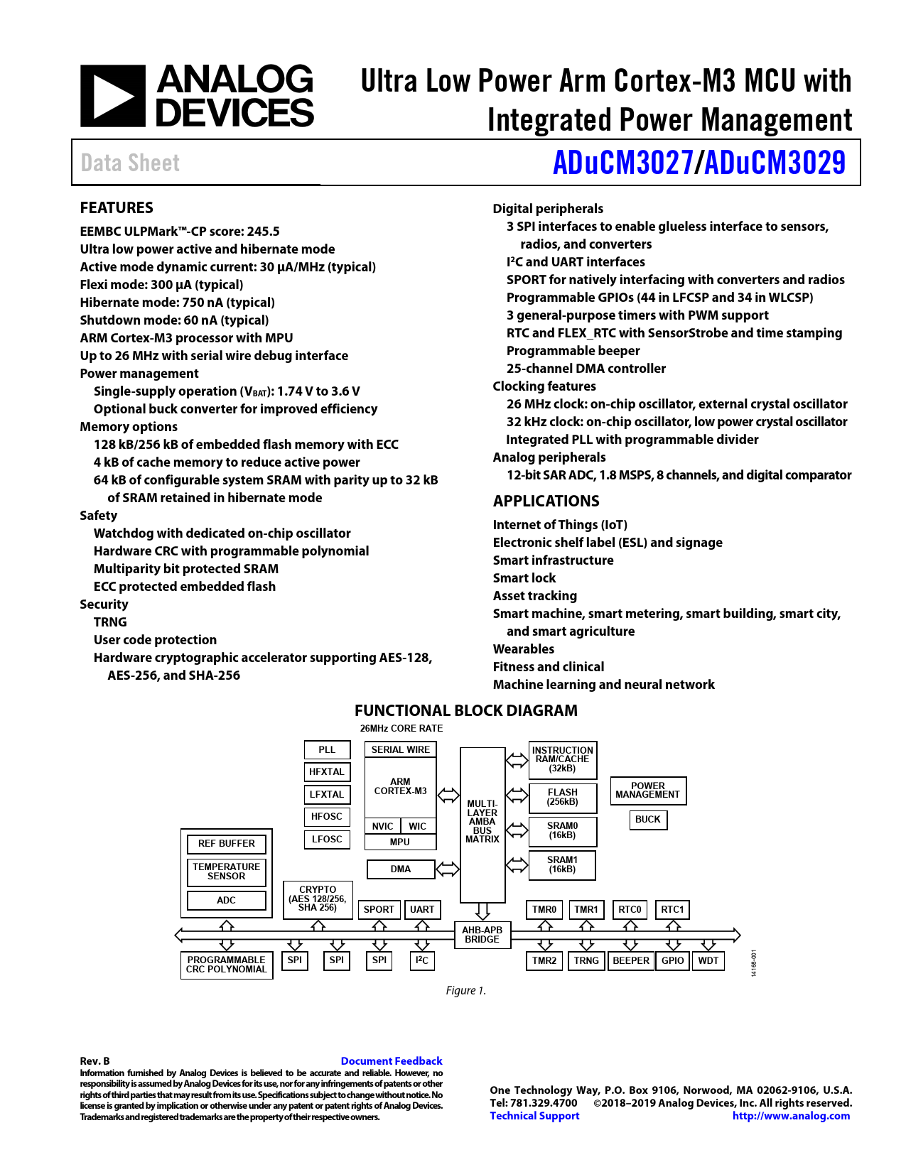
Ultra Low Power Arm Cortex-M3 MCU with Integrated Power Management Data Sheet ADuCM3027 /ADuCM3029 FEATURES Digital peripherals EEMBC ULPMark™-CP score: 245.5 3 SPI interfaces to enable glueless interface to sensors, Ultra low power active and hibernate mode radios, and converters Active mode dynamic current: 30 μA/MHz (typical) I2C and UART interfaces Flexi mode: 300 μA (typical) SPORT for natively interfacing with converters and radios Hibernate mode: 750 nA (typical) Programmable GPIOs (44 in LFCSP and 34 in WLCSP) Shutdown mode: 60 nA (typical) 3 general-purpose timers with PWM support ARM Cortex-M3 processor with MPU RTC and FLEX_RTC with SensorStrobe and time stamping Up to 26 MHz with serial wire debug interface Programmable beeper Power management 25-channel DMA controller Single-supply operation (V Clocking features BAT): 1.74 V to 3.6 V Optional buck converter for improved efficiency 26 MHz clock: on-chip oscillator, external crystal oscillator Memory options 32 kHz clock: on-chip oscillator, low power crystal oscillator 128 kB/256 kB of embedded flash memory with ECC Integrated PLL with programmable divider 4 kB of cache memory to reduce active power Analog peripherals 64 kB of configurable system SRAM with parity up to 32 kB 12-bit SAR ADC, 1.8 MSPS, 8 channels, and digital comparator of SRAM retained in hibernate mode APPLICATIONS Safety Internet of Things (IoT) Watchdog with dedicated on-chip oscillator Electronic shelf label (ESL) and signage Hardware CRC with programmable polynomial Smart infrastructure Multiparity bit protected SRAM Smart lock ECC protected embedded flash Asset tracking Security Smart machine, smart metering, smart building, smart city, TRNG and smart agriculture User code protection Wearables Hardware cryptographic accelerator supporting AES-128, Fitness and clinical AES-256, and SHA-256 Machine learning and neural network FUNCTIONAL BLOCK DIAGRAM 26MHz CORE RATE PLL SERIAL WIRE INSTRUCTION RAM/CACHE (32kB) HFXTAL ARM POWER CORTEX-M3 LFXTAL FLASH MANAGEMENT (256kB) MULTI- LAYER HFOSC AMBA BUCK NVIC WIC SRAM0 BUS (16kB) REF BUFFER LFOSC MPU MATRIX SRAM1 TEMPERATURE DMA (16kB) SENSOR CRYPTO ADC (AES 128/256, SHA 256) SPORT UART TMR0 TMR1 RTC0 RTC1 AHB-APB BRIDGE
01
PROGRAMMABLE SPI SPI SPI I2C TMR2 TRNG BEEPER GPIO WDT
-0
CRC POLYNOMIAL
168 14 Figure 1.
Rev. B Document Feedback Information furnished by Analog Devices is believed to be accurate and reliable. However, no responsibility is assumed by Analog Devices for its use, nor for any infringements of patents or other rights of third parties that may result from its use. Specifications subject to change without notice. No One Technology Way, P.O. Box 9106, Norwood, MA 02062-9106, U.S.A. license is granted by implication or otherwise under any patent or patent rights of Analog Devices. Tel: 781.329.4700 ©2018–2019 Analog Devices, Inc. All rights reserved. Trademarks and registered trademarks are the property of their respective owners. Technical Support http://www.analog.com
Document Outline Features Applications Functional Block Diagram Revision History General Description Product Highlights Specifications Operating Conditions and Electrical Characteristics Embedded Flash Specifications Power Supply Current Specifications Active Mode Flexi Mode Deep Sleep Modes—VBAT = 3.0 V ADC Specifications System Clocks External Crystal Oscillator Specifications On-Chip RC Oscillator Specifications System Clocks and PLL Specifications Timing Specifications Reset Timing Serial Ports Timing SPI Timing I2C Specifications General-Purpose Port Timing RTC1 (FLEX_RTC) Specifications Timer Pulse-Width Modulation (PWM) Output Cycle Timing Absolute Maximum Ratings Thermal Resistance ESD Caution Pin Configuration and Function Descriptions Typical Performance Characteristics Theory of Operation ARM Cortex-M3 Processor ARM Cortex-M3 Memory Subsystem Code Region SRAM Region System Region Memory Architecture SRAM Region MMRs (Peripheral Control and Status) Flash Memory Cache Controller System and Integration Features Reset Booting Power Management Power Modes Active Mode Flexi Mode Hibernate Mode Shutdown Mode Security Features Cryptographic Accelerator True Random Number Generator (TRNG) Reliability and Robustness Features ECC Enabled Flash Memory Multiparity Bit Protected SRAM Software Watchdog Cyclic Redundancy Check (CRC) Accelerator Programmable GPIOs Timers General-Purpose Timers Watchdog Timer (WDT) Analog-to-Digital Converter (ADC) Subsystem Clocking Beeper Driver Debug Capability On-Chip Peripheral Features Serial Ports (SPORT) SPI Ports UART Port I2C Development Support Documentation Hardware Software Additional Information Reference Designs MCU Test Conditions Driver Types EEMBC ULPMark™-CP Score GPIO Multiplexing Applications Information About ADuCM3027/ADuCM3029 Silicon Anomalies Functionality Issues Outline Dimensions Ordering Guide

 Купить ADUCM3029BCBZ-R7 на РадиоЛоцман.Цены — от 464 до 83 457 ₽