DatasheetsDatasheet ADA4528-1, ADA4528-2 (Analog …
Datasheet ADA4528-1, ADA4528-2 (Analog Devices)
| Производитель | Analog Devices |
| Описание | Precision, Ultralow Noise, RRIO, Zero-Drift Dual Op Amp |
| Страниц / Страница | 24 / 1 — Precision, Ultralow Noise, RRIO,. Zero-Drift Op Amp. Data Sheet. … |
| Версия | F |
| Формат / Размер файла | PDF / 701 Кб |
| Язык документа | английский |
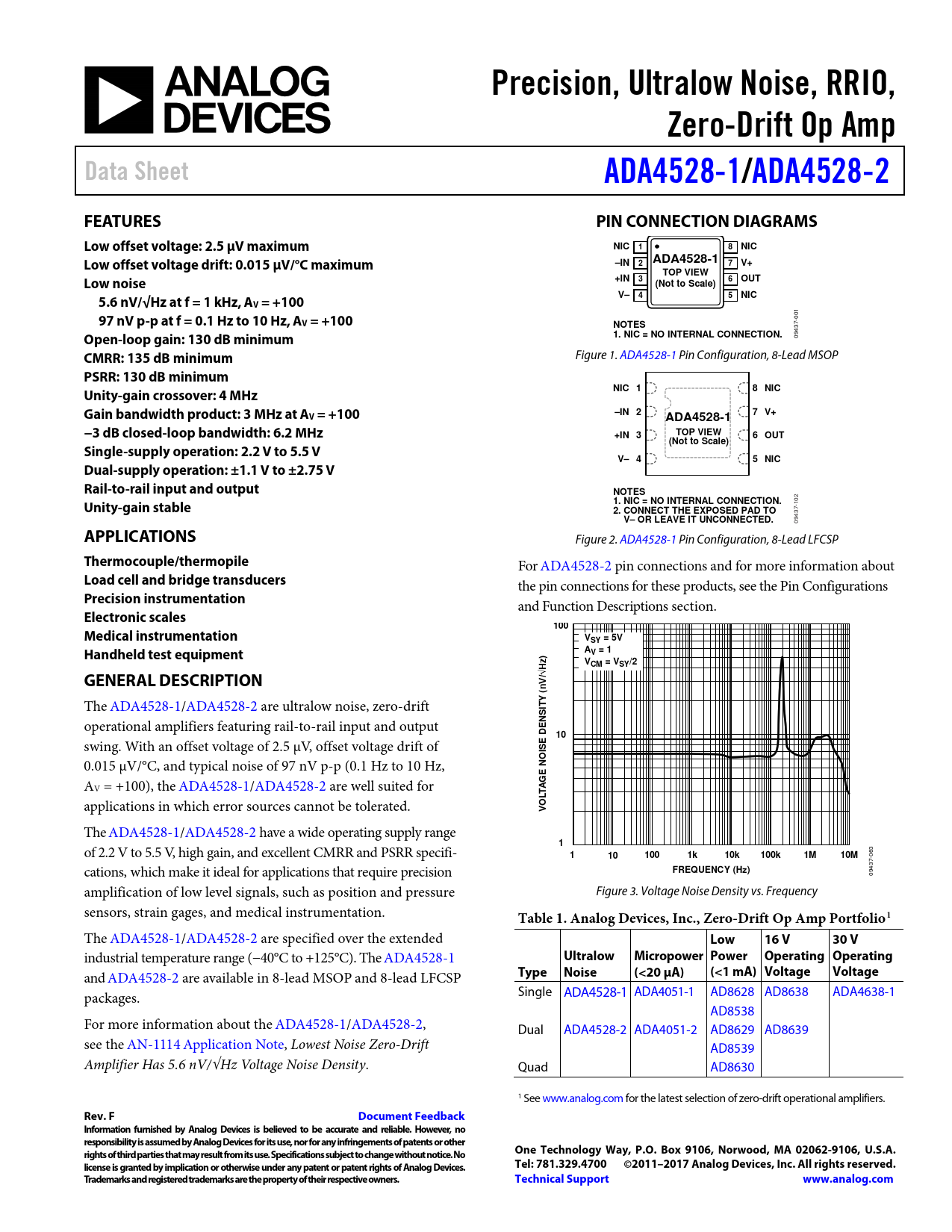
Precision, Ultralow Noise, RRIO,. Zero-Drift Op Amp. Data Sheet. ADA4528-1. /ADA4528-2. FEATURES. PIN CONNECTION DIAGRAMS

Модельный ряд для этого даташита
Текстовая версия документа
link to page 7 link to page 7 link to page 2
Precision, Ultralow Noise, RRIO, Zero-Drift Op Amp Data Sheet ADA4528-1 /ADA4528-2 FEATURES PIN CONNECTION DIAGRAMS Low offset voltage: 2.5 µV maximum NIC 1 8 NIC Low offset voltage drift: 0.015 μV/°C maximum –IN ADA4528-1 2 7 V+ TOP VIEW Low noise +IN 3 6 OUT (Not to Scale) 5.6 nV/√Hz at f = 1 kHz, A V– 4 5 NIC V = +100 97 nV p-p at f = 0.1 Hz to 10 Hz, A
001
V = +100 NOTES Open-loop gain: 130 dB minimum 1. NIC = NO INTERNAL CONNECTION.
09437-
CMRR: 135 dB minimum
Figure 1. ADA4528-1 Pin Configuration, 8-Lead MSOP
PSRR: 130 dB minimum Unity-gain crossover: 4 MHz NIC 1 8 NIC Gain bandwidth product: 3 MHz at AV = +100 –IN 2 ADA4528-1 7 V+ −3 dB closed-loop bandwidth: 6.2 MHz TOP VIEW +IN 3 6 OUT Single-supply operation: 2.2 V to 5.5 V (Not to Scale) V– 4 5 NIC Dual-supply operation: ±1.1 V to ±2.75 V Rail-to-rail input and output NOTES Unity-gain stable 1. NIC = NO INTERNAL CONNECTION.
102
2. CONNECT THE EXPOSED PAD TO V– OR LEAVE IT UNCONNECTED.
09437-
APPLICATIONS
Figure 2. ADA4528-1 Pin Configuration, 8-Lead LFCSP
Thermocouple/thermopile
For ADA4528-2 pin connections and for more information about
Load cell and bridge transducers
the pin connections for these products, see the Pin Configurations
Precision instrumentation
and Function Descriptions section.
Electronic scales Medical instrumentation 100 VSY = 5V Handheld test equipment AV = 1 z) VCM = VSY/2 GENERAL DESCRIPTION √H V/ (n
The ADA4528-1/ADA4528-2 are ultralow noise, zero-drift
Y T SI
operational amplifiers featuring rail-to-rail input and output
EN 10
swing. With an offset voltage of 2.5 μV, offset voltage drift of
ISE D
0.015 μV/°C, and typical noise of 97 nV p-p (0.1 Hz to 10 Hz,
O E N
A
G
V = +100), the ADA4528-1/ADA4528-2 are well suited for
A
applications in which error sources cannot be tolerated.
LT VO
The ADA4528-1/ADA4528-2 have a wide operating supply range of 2.2 V to 5.5 V, high gain, and excellent CMRR and PSRR specifi-
1 1 10 100 1k 10k 100k 1M 10M
063 cations, which make it ideal for applications that require precision
FREQUENCY (Hz)
09437- amplification of low level signals, such as position and pressure Figure 3. Voltage Noise Density vs. Frequency sensors, strain gages, and medical instrumentation.
Table 1. Analog Devices, Inc., Zero-Drift Op Amp Portfolio1
The ADA4528-1/ADA4528-2 are specified over the extended
Low 16 V 30 V
industrial temperature range (−40°C to +125°C). The ADA4528-1
Ultralow Micropower Power Operating Operating
and ADA4528-2 are available in 8-lead MSOP and 8-lead LFCSP
Type Noise (<20 µA) (<1 mA) Voltage Voltage
packages. Single ADA4528-1 ADA4051-1 AD8628 AD8638 ADA4638-1 AD8538 For more information about the ADA4528-1/ADA4528-2, Dual ADA4528-2 ADA4051-2 AD8629 AD8639 see the AN-1114 Application Note, Lowest Noise Zero-Drift AD8539 Amplifier Has 5.6 nV/√Hz Voltage Noise Density. Quad AD8630 1 See www.analog.com for the latest selection of zero-drift operational amplifiers.
Rev. F Document Feedback Information furnished by Analog Devices is believed to be accurate and reliable. However, no responsibility is assumed by Analog Devices for its use, nor for any infringements of patents or other rights of third parties that may result from its use. Specifications subject to change without notice. No One Technology Way, P.O. Box 9106, Norwood, MA 02062-9106, U.S.A. license is granted by implication or otherwise under any patent or patent rights of Analog Devices. Tel: 781.329.4700 ©2011–2017 Analog Devices, Inc. All rights reserved. Trademarks and registered trademarks are the property of their respective owners. Technical Support www.analog.com
Document Outline FEATURES APPLICATIONS GENERAL DESCRIPTION PIN CONNECTION DIAGRAMS TABLE OF CONTENTS REVISION HISTORY SPECIFICATIONS ELECTRICAL CHARACTERISTICS—2.5 V OPERATION ELECTRICAL CHARACTERISTICS—5 V OPERATION ABSOLUTE MAXIMUM RATINGS THERMAL RESISTANCE ESD CAUTION PIN CONFIGURATIONS AND FUNCTION DESCRIPTIONS TYPICAL PERFORMANCE CHARACTERISTICS APPLICATIONS INFORMATION INPUT PROTECTION RAIL-TO-RAIL INPUT AND OUTPUT NOISE CONSIDERATIONS 1/f Noise Source Resistance Voltage Noise Density with Different Gain Configurations Residual Voltage Ripple COMPARATOR OPERATION PRINTED CIRCUIT BOARD LAYOUT OUTLINE DIMENSIONS ORDERING GUIDE

 Купить ADA4528-1ACPZ-RL на РадиоЛоцман.Цены — от 44 до 588 ₽