Datasheet PT7C4563BQ (Diodes) - 4
| Производитель | Diodes |
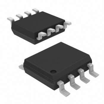
| Описание | Automotive Grade Real-time Clock |
| Страниц / Страница | 19 / 4 — PT7C4563BQ. Maximum Ratings. Note:. Recommended Operating Conditions. … |
| Формат / Размер файла | PDF / 1.0 Мб |
| Язык документа | английский |
PT7C4563BQ. Maximum Ratings. Note:. Recommended Operating Conditions. Symbol. Description. Min. Typ. Max. Unit

Модельный ряд для этого даташита
Текстовая версия документа
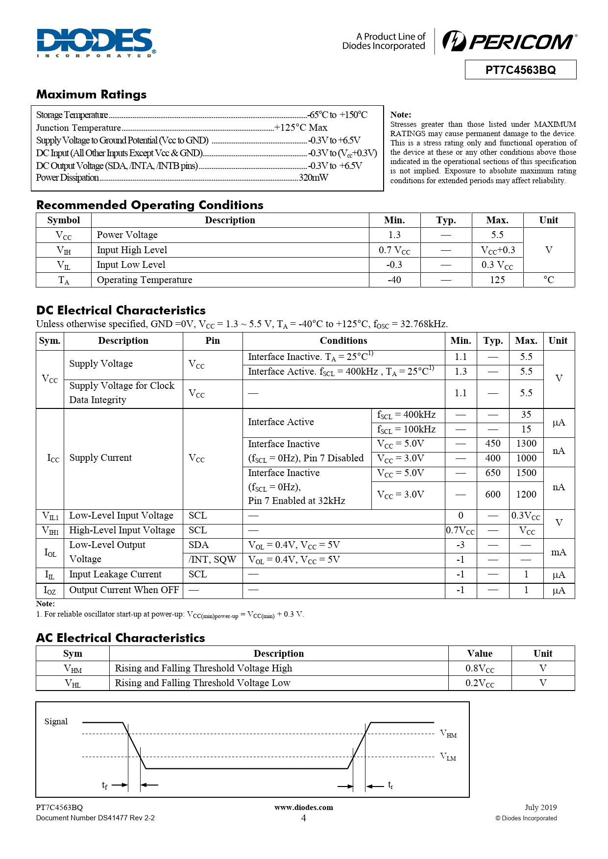
PT7C4563BQ Maximum Ratings
Storage Temperature .. -65°C to +150°C
Note:
Junction Temperature... +125°C Max Stresses greater than those listed under MAXIMUM RATINGS may cause permanent damage to the device. Supply Voltage to Ground Potential (Vcc to GND) .. -0.3V to +6.5V This is a stress rating only and functional operation of DC Input (All Other Inputs Except Vcc & GND)... -0.3V to (Vcc+0.3V) the device at these or any other conditions above those DC Output Voltage (SDA, /INTA, /INTB pins) ... -0.3V to +6.5V indicated in the operational sections of this specification Power Dissipation .. 320mW is not implied. Exposure to absolute maximum rating conditions for extended periods may affect reliability.
Recommended Operating Conditions Symbol Description Min. Typ. Max. Unit
VCC Power Voltage 1.3 — 5.5 VIH Input High Level 0.7 VCC — VCC+0.3 V VIL Input Low Level -0.3 — 0.3 VCC TA Operating Temperature -40 — 125 °C
DC Electrical Characteristics
Unless otherwise specified, GND =0V, VCC = 1.3 ~ 5.5 V, TA = -40°C to +125°C, fOSC = 32.768kHz.
Sym. Description Pin Conditions Min. Typ. Max. Unit
Interface Inactive. T Supply Voltage V A = 25°C1) 1.1 — 5.5 CC Interface Active. f V SCL = 400kHz , TA = 25°C1) 1.3 — 5.5 CC V Supply Voltage for Clock V Data Integrity CC — 1.1 — 5.5 f Interface Active SCL = 400kHz — — 35 µA fSCL = 100kHz — — 15 Interface Inactive VCC = 5.0V — 450 1300 nA ICC Supply Current VCC (fSCL = 0Hz), Pin 7 Disabled VCC = 3.0V — 400 1000 Interface Inactive VCC = 5.0V — 650 1500 (fSCL = 0Hz), nA V Pin 7 Enabled at 32kHz CC = 3.0V — 600 1200 VIL1 Low-Level Input Voltage SCL — 0 — 0.3VCC V VIH1 High-Level Input Voltage SCL — 0.7VCC — VCC Low-Level Output SDA V I OL = 0.4V, VCC = 5V -3 — — OL mA Voltage /INT, SQW VOL = 0.4V, VCC = 5V -1 — — IIL Input Leakage Current SCL — -1 — 1 µA IOZ Output Current When OFF — — -1 — 1 µA
Note:
1. For reliable oscillator start-up at power-up: VCC(min)power-up = VCC(min) + 0.3 V.
AC Electrical Characteristics Sym Description Value Unit
VHM Rising and Falling Threshold Voltage High 0.8VCC V VHL Rising and Falling Threshold Voltage Low 0.2VCC V Signal VHM VLM tf tr PT7C4563BQ
www.diodes.com
July 2019 Document Number DS41477 Rev 2-2 4 © Diodes Incorporated Document Outline Features Description Pin Configuration Pin Description Function Block Maximum Ratings Recommended Operating Conditions DC Electrical Characteristics AC Electrical Characteristics Recommended Layout for Crystal Cpar = all parasitical capacitor between X1 and X2 Crystal Specifications Function Description Overview of Functions Registers Control and Status Register Time Counter Days of the Week Counter Calendar Counter Communication I2C Bus Interface Overview of I2C Bus System Configuration Starting and Stopping I2C Bus Communications Slave Address Part Marking Packaging Mechanical W (SOIC-8)

 Купить PT7C4563BQ1WEX на РадиоЛоцман.Цены — от 46 до 8 668 ₽