Datasheet LT3757, LT3757A (Analog Devices) - 3
| Производитель | Analog Devices |
| Описание | Boost, Flyback, SEPIC and Inverting Controller |
| Страниц / Страница | 38 / 3 — ELECTRICAL CHARACTERISTICS. The. denotes the specifications which apply … |
| Версия | F |
| Формат / Размер файла | PDF / 1.3 Мб |
| Язык документа | английский |
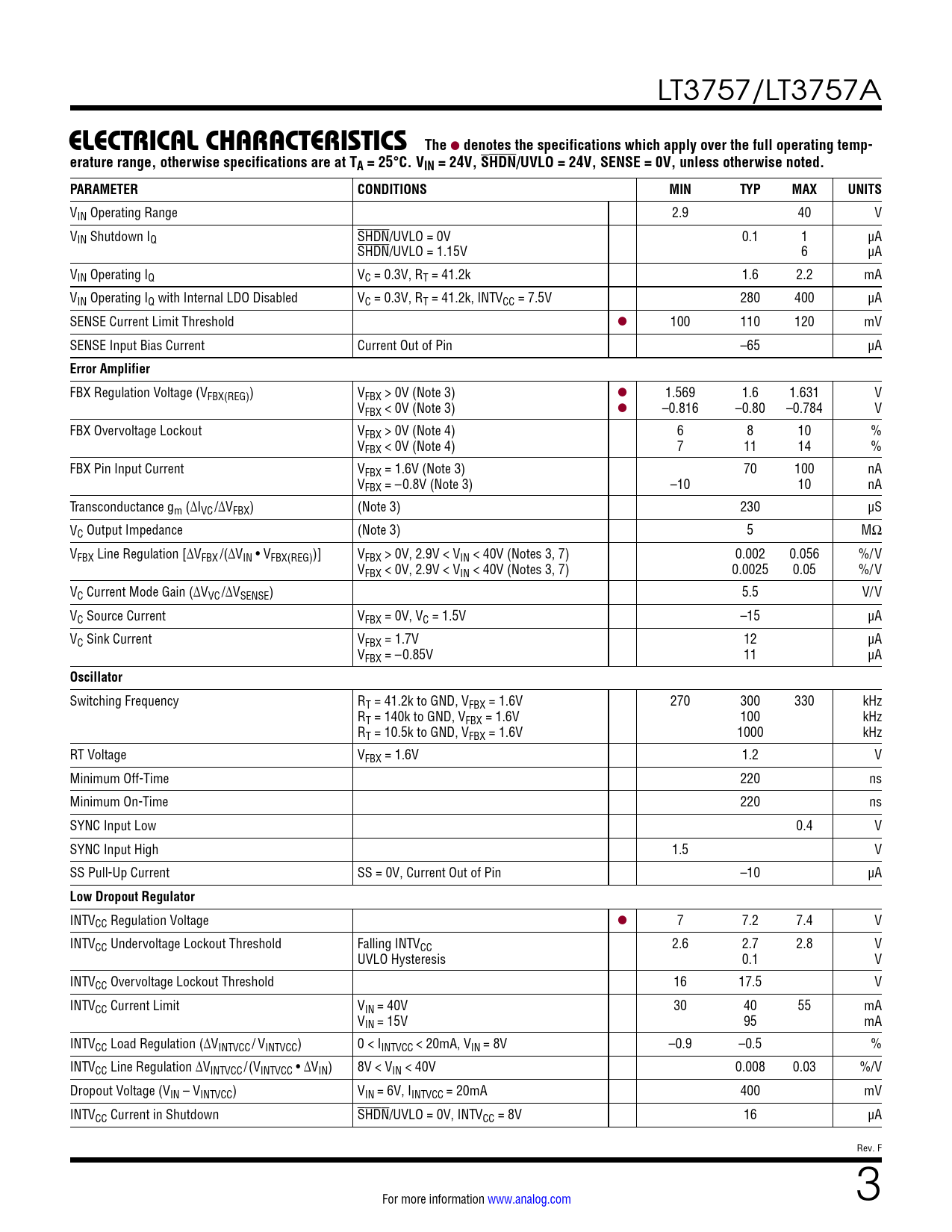
ELECTRICAL CHARACTERISTICS. The. denotes the specifications which apply over the full operating temp-
Модельный ряд для этого даташита
Текстовая версия документа
LT3757/LT3757A
ELECTRICAL CHARACTERISTICS The
l
denotes the specifications which apply over the full operating temp- erature range, otherwise specifications are at TA = 25°C. VIN = 24V, SHDN/UVLO = 24V, SENSE = 0V, unless otherwise noted. PARAMETER CONDITIONS MIN TYP MAX UNITS
VIN Operating Range 2.9 40 V VIN Shutdown IQ SHDN/UVLO = 0V 0.1 1 µA SHDN/UVLO = 1.15V 6 µA VIN Operating IQ VC = 0.3V, RT = 41.2k 1.6 2.2 mA VIN Operating IQ with Internal LDO Disabled VC = 0.3V, RT = 41.2k, INTVCC = 7.5V 280 400 µA SENSE Current Limit Threshold l 100 110 120 mV SENSE Input Bias Current Current Out of Pin –65 µA
Error Amplifier
FBX Regulation Voltage (VFBX(REG)) VFBX > 0V (Note 3) l 1.569 1.6 1.631 V VFBX < 0V (Note 3) l –0.816 –0.80 –0.784 V FBX Overvoltage Lockout VFBX > 0V (Note 4) 6 8 10 % VFBX < 0V (Note 4) 7 11 14 % FBX Pin Input Current VFBX = 1.6V (Note 3) 70 100 nA VFBX = –0.8V (Note 3) –10 10 nA Transconductance gm (∆IVC/∆VFBX) (Note 3) 230 µS VC Output Impedance (Note 3) 5 MΩ VFBX Line Regulation [∆VFBX/(∆VIN • VFBX(REG))] VFBX > 0V, 2.9V < VIN < 40V (Notes 3, 7) 0.002 0.056 %/V VFBX < 0V, 2.9V < VIN < 40V (Notes 3, 7) 0.0025 0.05 %/V VC Current Mode Gain (∆VVC/∆VSENSE) 5.5 V/V VC Source Current VFBX = 0V, VC = 1.5V –15 µA VC Sink Current VFBX = 1.7V 12 µA VFBX = –0.85V 11 µA
Oscillator
Switching Frequency RT = 41.2k to GND, VFBX = 1.6V 270 300 330 kHz RT = 140k to GND, VFBX = 1.6V 100 kHz RT = 10.5k to GND, VFBX = 1.6V 1000 kHz RT Voltage VFBX = 1.6V 1.2 V Minimum Off-Time 220 ns Minimum On-Time 220 ns SYNC Input Low 0.4 V SYNC Input High 1.5 V SS Pull-Up Current SS = 0V, Current Out of Pin –10 µA
Low Dropout Regulator
INTVCC Regulation Voltage l 7 7.2 7.4 V INTVCC Undervoltage Lockout Threshold Falling INTVCC 2.6 2.7 2.8 V UVLO Hysteresis 0.1 V INTVCC Overvoltage Lockout Threshold 16 17.5 V INTVCC Current Limit VIN = 40V 30 40 55 mA VIN = 15V 95 mA INTVCC Load Regulation (∆VINTVCC/ VINTVCC) 0 < IINTVCC < 20mA, VIN = 8V –0.9 –0.5 % INTVCC Line Regulation ∆VINTVCC/(VINTVCC • ∆VIN) 8V < VIN < 40V 0.008 0.03 %/V Dropout Voltage (VIN – VINTVCC) VIN = 6V, IINTVCC = 20mA 400 mV INTVCC Current in Shutdown SHDN/UVLO = 0V, INTVCC = 8V 16 µA Rev. F For more information www.analog.com 3 Document Outline Features Applications Typical Application Description Absolute Maximum Ratings Pin Configuration Order Information Electrical Characteristics Typical Performance Characteristics Pin Functions Block Diagram Applications Information Typical Applications Package Description Revision History Typical Application Related Parts

 Купить LT3757AMPMSE#TRPBF на РадиоЛоцман.Цены — от 284 до 895 ₽


