Datasheet AD9257-EP (Analog Devices)
| Производитель | Analog Devices |
| Описание | Octal, 14-Bit, 40/65 MSPS Serial LVDS 1.8 V A/D Converter |
| Страниц / Страница | 13 / 1 — Octal, 14-Bit, 65 MSPS, Serial LVDS,. 1.8 V Analog-to-Digital Converter. … |
| Версия | A |
| Формат / Размер файла | PDF / 300 Кб |
| Язык документа | английский |
Octal, 14-Bit, 65 MSPS, Serial LVDS,. 1.8 V Analog-to-Digital Converter. Data Sheet. AD9257-EP. FEATURES

Модельный ряд для этого даташита
Текстовая версия документа
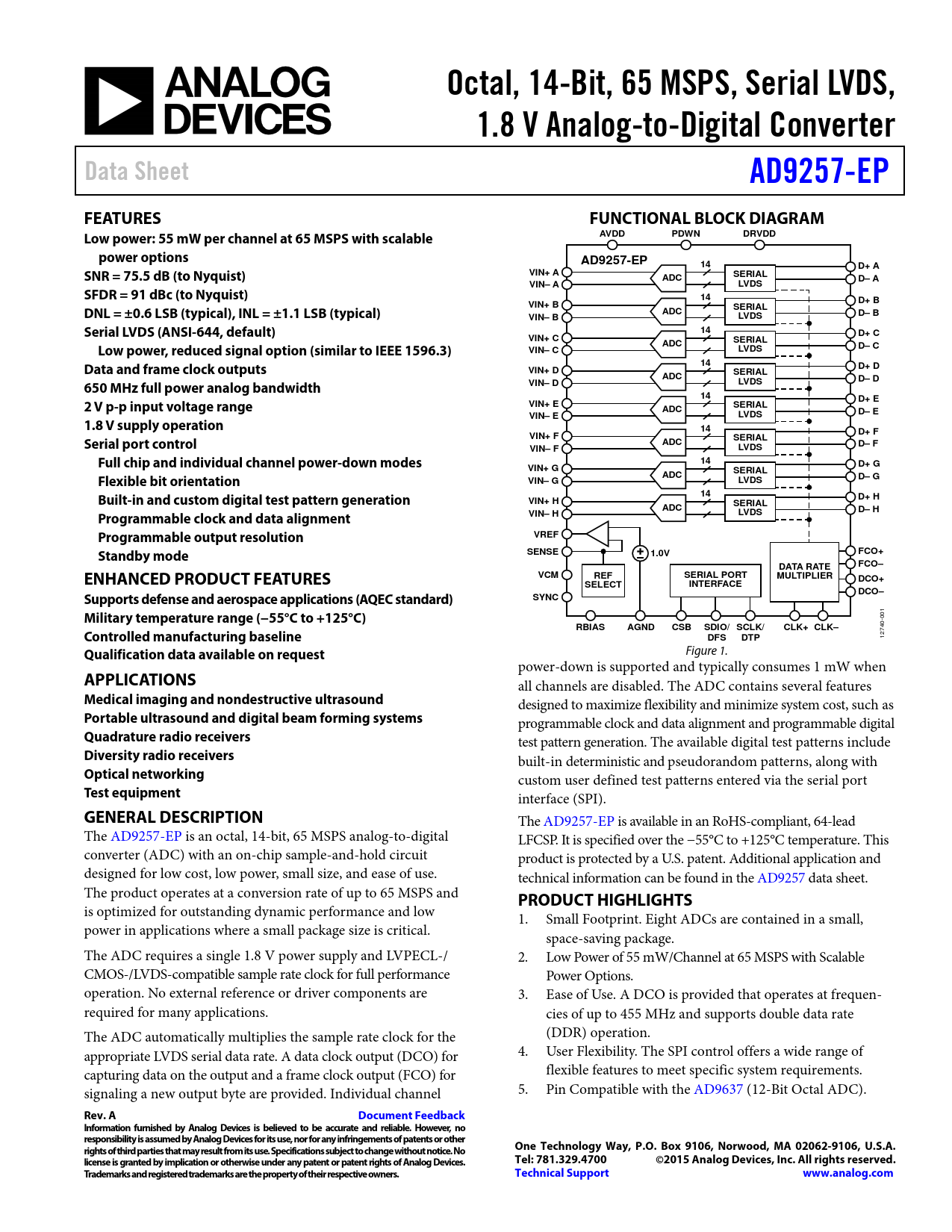
Octal, 14-Bit, 65 MSPS, Serial LVDS, 1.8 V Analog-to-Digital Converter Data Sheet AD9257-EP FEATURES FUNCTIONAL BLOCK DIAGRAM Low power: 55 mW per channel at 65 MSPS with scalable AVDD PDWN DRVDD power options AD9257-EP 14 D+ A SNR = 75.5 dB (to Nyquist) VIN+ A ADC SERIAL D– A VIN– A LVDS SFDR = 91 dBc (to Nyquist) 14 D+ B VIN+ B SERIAL DNL = ±0.6 LSB (typical), INL = ±1.1 LSB (typical) ADC D– B VIN– B LVDS Serial LVDS (ANSI-644, default) 14 D+ C VIN+ C ADC SERIAL Low power, reduced signal option (similar to IEEE 1596.3) LVDS D– C VIN– C 14 Data and frame clock outputs D+ D VIN+ D ADC SERIAL VIN– D LVDS D– D 650 MHz full power analog bandwidth 14 D+ E 2 V p-p input voltage range VIN+ E SERIAL ADC LVDS D– E VIN– E 1.8 V supply operation 14 D+ F VIN+ F SERIAL Serial port control ADC LVDS D– F VIN– F Full chip and individual channel power-down modes 14 D+ G VIN+ G ADC SERIAL Flexible bit orientation VIN– G LVDS D– G 14 Built-in and custom digital test pattern generation D+ H VIN+ H ADC SERIAL VIN– H LVDS D– H Programmable clock and data alignment Programmable output resolution VREF Standby mode SENSE FCO+ 1.0V DATA RATE FCO– ENHANCED PRODUCT FEATURES VCM REF SERIAL PORT MULTIPLIER DCO+ SELECT INTERFACE DCO– Supports defense and aerospace applications (AQEC standard) SYNC
1
Military temperature range (−55°C to +125°C)
00 0-
RBIAS AGND CSB SDIO/ SCLK/ CLK+ CLK–
74
Controlled manufacturing baseline DFS DTP
12
Qualification data available on request
Figure 1. power-down is supported and typically consumes 1 mW when
APPLICATIONS
all channels are disabled. The ADC contains several features
Medical imaging and nondestructive ultrasound
designed to maximize flexibility and minimize system cost, such as
Portable ultrasound and digital beam forming systems
programmable clock and data alignment and programmable digital
Quadrature radio receivers
test pattern generation. The available digital test patterns include
Diversity radio receivers
built-in deterministic and pseudorandom patterns, along with
Optical networking
custom user defined test patterns entered via the serial port
Test equipment
interface (SPI).
GENERAL DESCRIPTION
The AD9257-EP is available in an RoHS-compliant, 64-lead The AD9257-EP is an octal, 14-bit, 65 MSPS analog-to-digital LFCSP. It is specified over the −55°C to +125°C temperature. This converter (ADC) with an on-chip sample-and-hold circuit product is protected by a U.S. patent. Additional application and designed for low cost, low power, small size, and ease of use. technical information can be found in the AD9257 data sheet. The product operates at a conversion rate of up to 65 MSPS and
PRODUCT HIGHLIGHTS
is optimized for outstanding dynamic performance and low 1. Small Footprint. Eight ADCs are contained in a small, power in applications where a small package size is critical. space-saving package. The ADC requires a single 1.8 V power supply and LVPECL-/ 2. Low Power of 55 mW/Channel at 65 MSPS with Scalable CMOS-/LVDS-compatible sample rate clock for full performance Power Options. operation. No external reference or driver components are 3. Ease of Use. A DCO is provided that operates at frequen- required for many applications. cies of up to 455 MHz and supports double data rate The ADC automatically multiplies the sample rate clock for the (DDR) operation. appropriate LVDS serial data rate. A data clock output (DCO) for 4. User Flexibility. The SPI control offers a wide range of capturing data on the output and a frame clock output (FCO) for flexible features to meet specific system requirements. signaling a new output byte are provided. Individual channel 5. Pin Compatible with the AD9637 (12-Bit Octal ADC).
Rev. A Document Feedback Information furnished by Analog Devices is believed to be accurate and reliable. However, no responsibility is assumed by Analog Devices for its use, nor for any infringements of patents or other rights of third parties that may result from its use. Specifications subject to change without notice. No One Technology Way, P.O. Box 9106, Norwood, MA 02062-9106, U.S.A. license is granted by implication or otherwise under any patent or patent rights of Analog Devices. Tel: 781.329.4700 ©2015 Analog Devices, Inc. All rights reserved. Trademarks and registered trademarks are the property of their respective owners. Technical Support www.analog.com
Document Outline FEATURES ENHANCED PRODUCT FEATURES APPLICATIONS GENERAL DESCRIPTION FUNCTIONAL BLOCK DIAGRAM PRODUCT HIGHLIGHTS TABLE OF CONTENTS REVISION HISTORY SPECIFICATIONS DC SPECIFICATIONS AC SPECIFICATIONS DIGITAL SPECIFICATIONS SWITCHING SPECIFICATIONS TIMING SPECIFICATIONS Timing Diagrams ABSOLUTE MAXIMUM RATINGS THERMAL CHARACTERISTICS ESD CAUTION PIN CONFIGURATION AND FUNCTION DESCRIPTIONS TYPICAL PERFORMANCE CHARACTERISTICS OUTLINE DIMENSIONS ORDERING GUIDE
 Купить AD9257BCPZRL7-40 на РадиоЛоцман.Цены — от 3 840 до 449 224 ₽