Datasheet AD7949-EP (Analog Devices)
| Производитель | Analog Devices |
| Описание | 14-Bit, 8-Channel, 250 kSPS PulSAR ADC |
| Страниц / Страница | 12 / 1 — 14-Bit, 8-Channel,. 250 kSPS PulSAR ADC. Enhanced Product. AD7949-EP. … |
| Версия | B |
| Формат / Размер файла | PDF / 318 Кб |
| Язык документа | английский |
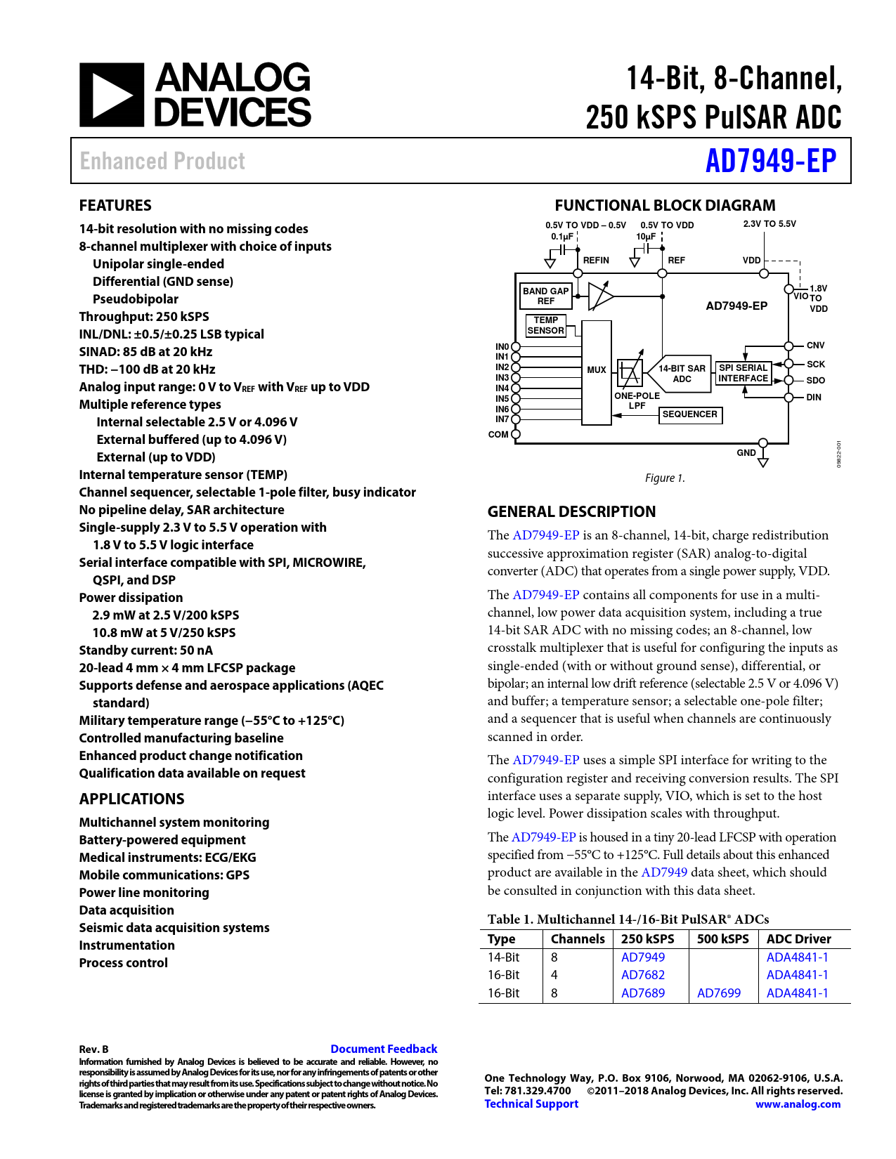
14-Bit, 8-Channel,. 250 kSPS PulSAR ADC. Enhanced Product. AD7949-EP. FEATURES. FUNCTIONAL BLOCK DIAGRAM

Модельный ряд для этого даташита
Текстовая версия документа
14-Bit, 8-Channel, 250 kSPS PulSAR ADC Enhanced Product AD7949-EP FEATURES FUNCTIONAL BLOCK DIAGRAM 14-bit resolution with no missing codes 0.5V TO VDD – 0.5V 0.5V TO VDD 2.3V TO 5.5V 0.1µF 10µF 8-channel multiplexer with choice of inputs Unipolar single-ended REFIN REF VDD Differential (GND sense) 1.8V BAND GAP Pseudobipolar VIO TO REF AD7949-EP VDD Throughput: 250 kSPS TEMP INL/DNL: ±0.5/±0.25 LSB typical SENSOR IN0 CNV SINAD: 85 dB at 20 kHz IN1 THD: −100 dB at 20 kHz SCK IN2 SPI SERIAL MUX 14-BIT SAR IN3 ADC INTERFACE SDO Analog input range: 0 V to VREF with VREF up to VDD IN4 IN5 ONE-POLE DIN Multiple reference types IN6 LPF SEQUENCER Internal selectable 2.5 V or 4.096 V IN7 External buffered (up to 4.096 V) COM
001
External (up to VDD) GND
9822- 0
Internal temperature sensor (TEMP)
Figure 1.
Channel sequencer, selectable 1-pole filter, busy indicator No pipeline delay, SAR architecture GENERAL DESCRIPTION Single-supply 2.3 V to 5.5 V operation with
The AD7949-EP is an 8-channel, 14-bit, charge redistribution
1.8 V to 5.5 V logic interface
successive approximation register (SAR) analog-to-digital
Serial interface compatible with SPI, MICROWIRE,
converter (ADC) that operates from a single power supply, VDD.
QSPI, and DSP Power dissipation
The AD7949-EP contains all components for use in a multi-
2.9 mW at 2.5 V/200 kSPS
channel, low power data acquisition system, including a true
10.8 mW at 5 V/250 kSPS
14-bit SAR ADC with no missing codes; an 8-channel, low
Standby current: 50 nA
crosstalk multiplexer that is useful for configuring the inputs as
20-lead 4 mm × 4 mm LFCSP package
single-ended (with or without ground sense), differential, or
Supports defense and aerospace applications (AQEC
bipolar; an internal low drift reference (selectable 2.5 V or 4.096 V)
standard)
and buffer; a temperature sensor; a selectable one-pole filter;
Military temperature range (−55°C to +125°C)
and a sequencer that is useful when channels are continuously
Controlled manufacturing baseline
scanned in order.
Enhanced product change notification
The AD7949-EP uses a simple SPI interface for writing to the
Qualification data available on request
configuration register and receiving conversion results. The SPI
APPLICATIONS
interface uses a separate supply, VIO, which is set to the host logic level. Power dissipation scales with throughput.
Multichannel system monitoring Battery-powered equipment
The AD7949-EP is housed in a tiny 20-lead LFCSP with operation
Medical instruments: ECG/EKG
specified from −55°C to +125°C. Full details about this enhanced
Mobile communications: GPS
product are available in the AD7949 data sheet, which should
Power line monitoring
be consulted in conjunction with this data sheet.
Data acquisition Table 1. Multichannel 14-/16-Bit PulSAR® ADCs Seismic data acquisition systems Type Channels 250 kSPS 500 kSPS ADC Driver Instrumentation Process control
14-Bit 8 AD7949 ADA4841-1 16-Bit 4 AD7682 ADA4841-1 16-Bit 8 AD7689 AD7699 ADA4841-1
Rev. B Document Feedback Information furnished by Analog Devices is believed to be accurate and reliable. However, no responsibility is assumed by Analog Devices for its use, nor for any infringements of patents or other One Technology Way, P.O. Box 9106, Norwood, MA 02062-9106, U.S.A. rights of third parties that may result from its use. Specifications subject to change without notice. No license is granted by implication or otherwise under any patent or patent rights of Analog Devices. Tel: 781.329.4700 ©2011–2018 Analog Devices, Inc. All rights reserved. Trademarks and registered trademarks are the property of their respective owners. Technical Support www.analog.com
Document Outline Features Applications Functional Block Diagram General Description Table of Contents Revision History Specifications Timing Specifications Absolute Maximum Ratings ESD Caution Pin Configuration and Function Descriptions Typical Performance Characteristics Outline Dimensions Ordering Guide
 Купить AD7949SCPZ-EP-R2 на РадиоЛоцман.Цены — от 418 до 191 101 ₽