DatasheetsDatasheet ADuM4120/ADuM4120-1 (Analog Devices)
Datasheet ADuM4120/ADuM4120-1 (Analog Devices)
| Производитель | Analog Devices |
| Описание | Isolated, Precision Gate Driver with 2 A Output |
| Страниц / Страница | 17 / 1 — Isolated, Precision Gate Drivers. with 2 A Output. Data Sheet. ADuM4120/. … |
| Формат / Размер файла | PDF / 309 Кб |
| Язык документа | английский |
Isolated, Precision Gate Drivers. with 2 A Output. Data Sheet. ADuM4120/. ADuM4120-1. FEATURES. GENERAL DESCRIPTION

Модельный ряд для этого даташита
Текстовая версия документа
Isolated, Precision Gate Drivers with 2 A Output Data Sheet ADuM4120/ ADuM4120-1 FEATURES GENERAL DESCRIPTION 2.3 A peak output current (<2 Ω RDSON_x)
The ADuM4120/ADuM4120-11 are 2 A isolated, single-channel
2.5 V to 6.5 V VDD1 input
drivers that employ Analog Devices, Inc., iCoupler® technology
4.5V to 35 V VDD2 output
to provide precision isolation. The ADuM4120/ADuM4120-1
UVLO at 2.3 V VDD1
provide 5 kV rms isolation in the 6-lead wide body SOIC package
Multiple UVLO options on VDD2
with increased creepage. Combining high speed CMOS and
Grade A—4.4 V (typical) positive going threshold
monolithic transformer technology, these isolation components
Grade B—7.3 V (typical) positive going threshold
provide outstanding performance characteristics, such as the
Grade C—11.3 V (typical) positive going threshold
combination of pulse transformers and gate drivers.
Precise timing characteristics
The ADuM4120/ADuM4120-1 operate with input supplies
79 ns maximum isolator and driver propagation delay
ranging from 2.5 V to 6.5 V, providing compatibility with lower
falling edge (ADuM4120)
voltage systems. In comparison to gate drivers employing
CMOS input logic levels
high voltage level translation methodologies, the ADuM4120/
High common-mode transient immunity: 150 kV/μs
ADuM4120-1 offer the benefit of true, galvanic isolation between
High junction temperature operation: 125°C
the input and the output.
Default low output Safety and regulatory approvals (pending)
Options exist for models with and without an input glitch filter.
UL recognition per UL 1577
The glitch filter helps reduce the chance of noise on the input pin
5 kV rms for 1 minute SOIC long package
triggering an output.
CSA Component Acceptance Notice 5A
As a result, the ADuM4120/ADuM4120-1 provide reliable
VDE certificate of conformity (pending)
control over the switching characteristics of insulated gate
DIN V VDE V 0884-10 (VDE V 0884-10):2006-12
bipolar transistor (IGBT)/metal-oxide semiconductor field effect
VIORM = 849 V peak
transistor (MOSFET) configurations over a wide range of
8 mm creepage
switching voltages.
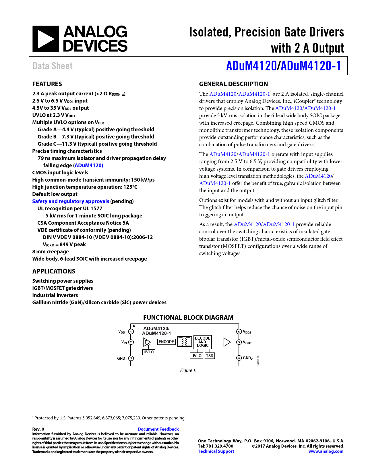
Wide body, 6-lead SOIC with increased creepage APPLICATIONS Switching power supplies IGBT/MOSFET gate drivers Industrial inverters Gallium nitride (GaN)/silicon carbide (SiC) power devices FUNCTIONAL BLOCK DIAGRAM ADuM4120/ VDD1 1 6 VDD2 ADuM4120-1 DECODE V 2 ENCODE AND IN 5 VOUT LOGIC UVLO UVLO TSD GND 3 4 GND
001
1 2
93- 154 Figure 1. 1 Protected by U.S. Patents 5,952,849; 6,873,065; 7,075,239. Other patents pending.
Rev. 0 Document Feedback Information furnished by Analog Devices is believed to be accurate and reliable. However, no responsibility is assumed by Analog Devices for its use, nor for any infringements of patents or other rights of third parties that may result from its use. Specifications subject to change without notice. No One Technology Way, P.O. Box 9106, Norwood, MA 02062-9106, U.S.A. license is granted by implication or otherwise under any patent or patent rights of Analog Devices. Tel: 781.329.4700 ©2017 Analog Devices, Inc. All rights reserved. Trademarks and registered trademarks are the property of their respective owners. Technical Support www.analog.com
Document Outline FEATURES APPLICATIONS GENERAL DESCRIPTION FUNCTIONAL BLOCK DIAGRAM TABLE OF CONTENTS REVISION HISTORY SPECIFICATIONS ELECTRICAL CHARACTERISTICS REGULATORY INFORMATION PACKAGE CHARACTERISTICS INSULATION AND SAFETY RELATED SPECIFICATIONS DIN V VDE V 0884-10 (VDE V 0884-10) INSULATION CHARACTERISTICS RECOMMENDED OPERATING CONDITIONS ABSOLUTE MAXIMUM RATINGS ESD CAUTION PIN CONFIGURATION AND FUNCTION DESCRIPTIONS TYPICAL PERFORMANCE CHARACTERISTICS THEORY OF OPERATION APPLICATIONS INFORMATION PCB LAYOUT PROPAGATION DELAY RELATED PARAMETERS THERMAL LIMITATIONS AND SWITCH LOAD CHARACTERISTICS UNDERVOLTAGE LOCKOUT (UVLO) OUTPUT LOAD CHARACTERISTICS POWER DISSIPATION DC CORRECTNESS AND MAGNETIC FIELD IMMUNITY INSULATION LIFETIME Surface Tracking Insulation Wear Out Calculation and Use of Parameters Example OUTLINE DIMENSIONS ORDERING GUIDE
 Купить ADUM4120-1ARIZ-RL на РадиоЛоцман.Цены — от 243 до 12 411 ₽