Datasheet ADL5601 (Analog Devices)
| Производитель | Analog Devices |
| Описание | 50 MHz TO 4.0 GHz RF/IF Gain Block |
| Страниц / Страница | 16 / 1 — 50 MHz to 4.0 GHz. RF/IF Gain Block. Data Sheet. ADL5601. FEATURES. … |
| Версия | A |
| Формат / Размер файла | PDF / 323 Кб |
| Язык документа | английский |
50 MHz to 4.0 GHz. RF/IF Gain Block. Data Sheet. ADL5601. FEATURES. FUNCTIONAL BLOCK DIAGRAM. Fixed gain of 15 dB. GND

Модельный ряд для этого даташита
Текстовая версия документа
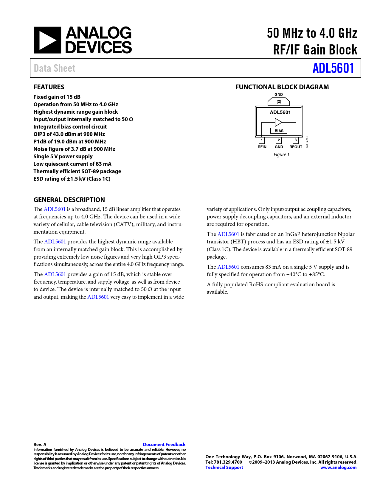
50 MHz to 4.0 GHz RF/IF Gain Block Data Sheet ADL5601 FEATURES FUNCTIONAL BLOCK DIAGRAM Fixed gain of 15 dB GND Operation from 50 MHz to 4.0 GHz (2) Highest dynamic range gain block ADL5601 Input/output internally matched to 50 Ω Integrated bias control circuit BIAS OIP3 of 43.0 dBm at 900 MHz P1dB of 19.0 dBm at 900 MHz 1 2 3
001
Noise figure of 3.7 dB at 900 MHz RFIN GND RFOUT
08219-
Single 5 V power supply
Figure 1.
Low quiescent current of 83 mA Thermally efficient SOT-89 package ESD rating of ±1.5 kV (Class 1C) GENERAL DESCRIPTION
The ADL5601 is a broadband, 15 dB linear amplifier that operates variety of applications. Only input/output ac coupling capacitors, at frequencies up to 4.0 GHz. The device can be used in a wide power supply decoupling capacitors, and an external inductor variety of cellular, cable television (CATV), military, and instru- are required for operation. mentation equipment. The ADL5601 is fabricated on an InGaP heterojunction bipolar The ADL5601 provides the highest dynamic range available transistor (HBT) process and has an ESD rating of ±1.5 kV from an internally matched gain block. This is accomplished by (Class 1C). The device is available in a thermal y efficient SOT-89 providing extremely low noise figures and very high OIP3 speci- package. fications simultaneously, across the entire 4.0 GHz frequency range. The ADL5601 consumes 83 mA on a single 5 V supply and is The ADL5601 provides a gain of 15 dB, which is stable over fully specified for operation from −40°C to +85°C. frequency, temperature, and supply voltage, as wel as from device A fully populated RoHS-compliant evaluation board is to device. The device is internally matched to 50 Ω at the input available. and output, making the ADL5601 very easy to implement in a wide
Rev. A Document Feedback Information furnished by Analog Devices is believed to be accurate and reliable. However, no responsibility is assumed by Analog Devices for its use, nor for any infringements of patents or other rights of third parties that may result from its use. Specifications subject to change without notice. No One Technology Way, P.O. Box 9106, Norwood, MA 02062-9106, U.S.A. license is granted by implication or otherwise under any patent or patent rights of Analog Devices. Tel: 781.329.4700 ©2009–2013 Analog Devices, Inc. All rights reserved. Trademarks and registered trademarks are the property of their respective owners. Technical Support www.analog.com
Document Outline Features Functional Block Diagram General Description Revision History Specifications Typical Scattering Parameters (S-Parameters) Absolute Maximum Ratings ESD Caution Pin Configuration and Function Descriptions Typical Performance Characteristics Basic Connections Soldering Information and Recommended PCB Land Pattern W-CDMA ACPR Performance Evaluation Board Outline Dimensions Ordering Guide

 Купить ADL5601ARKZ-R7 на РадиоЛоцман.Цены — от 134 до 20 529 ₽