DatasheetsDatasheet ADSP-21362, ADSP-21363, ADSP-21364, …
Datasheet ADSP-21362, ADSP-21363, ADSP-21364, ADSP-21365, ADSP-21366 (Analog Devices)
| Производитель | Analog Devices |
| Описание | SHARC Processors |
| Страниц / Страница | 60 / 1 — SHARC Processors. ADSP-21362/ADSP-21363/ADSP-. … |
| Версия | J |
| Формат / Размер файла | PDF / 1.4 Мб |
| Язык документа | английский |
SHARC Processors. ADSP-21362/ADSP-21363/ADSP-. 21364/ADSP-21365/ADSP-21366. SUMMARY. DEDICATED AUDIO COMPONENTS

Модельный ряд для этого даташита
Текстовая версия документа
link to page 56 link to page 56
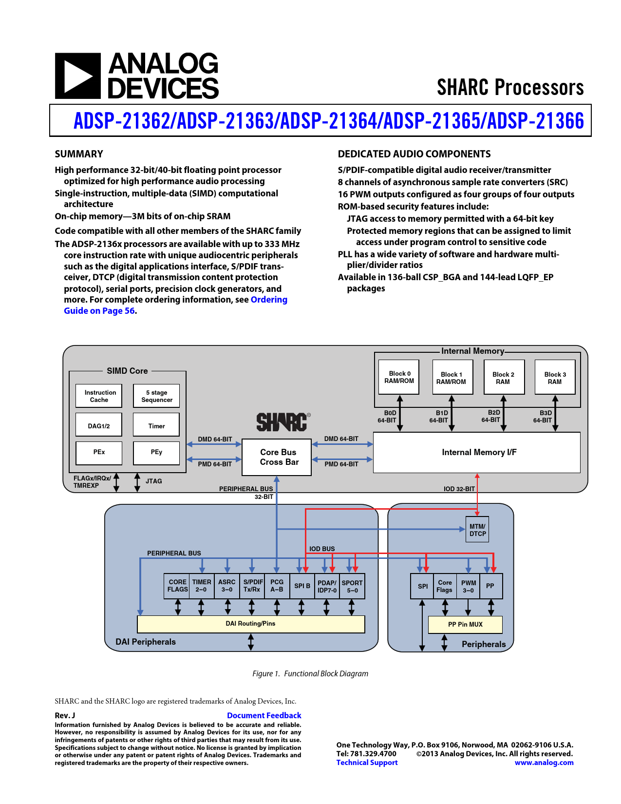
SHARC Processors ADSP-21362/ADSP-21363/ADSP- 21364/ADSP-21365/ADSP-21366 SUMMARY DEDICATED AUDIO COMPONENTS High performance 32-bit/40-bit floating point processor S/PDIF-compatible digital audio receiver/transmitter optimized for high performance audio processing 8 channels of asynchronous sample rate converters (SRC) Single-instruction, multiple-data (SIMD) computational 16 PWM outputs configured as four groups of four outputs architecture ROM-based security features include: On-chip memory—3M bits of on-chip SRAM JTAG access to memory permitted with a 64-bit key Code compatible with all other members of the SHARC family Protected memory regions that can be assigned to limit The ADSP-2136x processors are available with up to 333 MHz access under program control to sensitive code core instruction rate with unique audiocentric peripherals PLL has a wide variety of software and hardware multi- such as the digital applications interface, S/PDIF trans- plier/divider ratios ceiver, DTCP (digital transmission content protection Available in 136-ball CSP_BGA and 144-lead LQFP_EP protocol), serial ports, precision clock generators, and packages more. For complete ordering information, see Ordering Guide on Page 56 . Internal Memory SIMD Core Block 0 Block 1 Block 2 Block 3 RAM/ROM RAM/ROM RAM RAM Instruction 5 stage Cache Sequencer B0D B1D B2D B3D 64-BIT 64-BIT 64-BIT 64-BIT
S
DAG1/2 Timer DMD 64-BIT DMD 64-BIT PEx PEy Core Bus Internal Memory I/F PMD 64-BIT Cross Bar PMD 64-BIT FLAGx/IRQx/ JTAG TMREXP PERIPHERAL BUS IOD 32-BIT 32-BIT MTM/ DTCP IOD BUS PERIPHERAL BUS CORE TIMER ASRC S/PDIF PCG PDAP/ Core PWM SPI B SPORT SPI PP FLAGS 2-0 3-0 Tx/Rx A-B IDP7-0 5-0 Flags 3-0 DAI Routing/Pins PP Pin MUX DAI Peripherals Peripherals
Figure 1. Functional Block Diagram SHARC and the SHARC logo are registered trademarks of Analog Devices, Inc.
Rev. J Document Feedback Information furnished by Analog Devices is believed to be accurate and reliable. However, no responsibility is assumed by Analog Devices for its use, nor for any infringements of patents or other rights of third parties that may result from its use. Specifications subject to change without notice. No license is granted by implication One Technology Way, P.O. Box 9106, Norwood, MA 02062-9106 U.S.A. or otherwise under any patent or patent rights of Analog Devices. Trademarks and Tel: 781.329.4700 ©2013 Analog Devices, Inc. All rights reserved. registered trademarks are the property of their respective owners. Technical Support www.analog.com
Document Outline Summary Dedicated Audio Components Table of Contents Revision History General Description SHARC Family Core Architecture SIMD Computational Engine Independent, Parallel Computation Units Data Register File Context Switch Universal Registers Timer Single-Cycle Fetch of Instruction and Four Operands Instruction Cache Data Address Generators with Zero-Overhead Hardware Circular Buffer Support Flexible Instruction Set On-Chip Memory On-Chip Memory Bandwidth ROM-Based Security Family Peripheral Architecture Parallel Port Serial Peripheral (Compatible) Interface Pulse-Width Modulation Digital Audio Interface (DAI) Serial Ports S/PDIF-Compatible Digital Audio Receiver/Transmitter Digital Transmission Content Protection (DTCP) Memory-to-Memory (MTM) Synchronous/Asynchronous Sample Rate Converter (SRC) Input Data Port (IDP) Precision Clock Generator (PCG) Peripheral Timers I/O Processor Features DMA Controller System Design Program Booting Phase-Locked Loop Power Supplies Target Board JTAG Emulator Connector Development Tools Integrated Development Environments (IDEs) EZ-KIT Lite Evaluation Board EZ-KIT Lite Evaluation Kits Software Add-Ins for CrossCore Embedded Studio Board Support Packages for Evaluation Hardware Middleware Packages Algorithmic Modules Designing an Emulator-Compatible DSP Board (Target) Additional Information Related Signal Chains Pin Function Descriptions Specifications Operating Conditions Electrical Characteristics Package Information ESD Caution Maximum Power Dissipation Absolute Maximum Ratings Timing Specifications Core Clock Requirements Voltage Controlled Oscillator Power-Up Sequencing Clock Input Clock Signals Reset Interrupts Core Timer Timer PWM_OUT Cycle Timing Timer WDTH_CAP Timing DAI Pin to Pin Direct Routing Precision Clock Generator (Direct Pin Routing) Flags Memory Read—Parallel Port Memory Write—Parallel Port Serial Ports Input Data Port (IDP) Parallel Data Acquisition Port (PDAP) Pulse-Width Modulation Generators Sample Rate Converter—Serial Input Port Sample Rate Converter—Serial Output Port S/PDIF Transmitter S/PDIF Transmitter-Serial Input Waveforms S/PDIF Transmitter Input Data Timing Oversampling Clock (TxCLK) Switching Characteristics S/PDIF Receiver Internal Digital PLL Mode SPI Interface—Master SPI Interface—Slave JTAG Test Access Port and Emulation Output Drive Currents Test Conditions Capacitive Loading Thermal Characteristics 144-Lead LQFP_EP Pin Configurations 136-Ball BGA Pin Configurations Package Dimensions Surface-Mount Design Automotive Products Ordering Guide

 Купить ADSP-21363KBCZ-1AA на РадиоЛоцман.Цены — от 110 до 7 416 ₽