Datasheet LT8708 (Analog Devices) - 6
| Производитель | Analog Devices |
| Описание | 80V Synchronous 4-Switch Buck-Boost DC/DC Controller with Bidirectional Capability |
| Страниц / Страница | 64 / 6 — ELECTRICAL CHARACTERISTICS. The. denotes the specifications which apply … |
| Версия | A |
| Формат / Размер файла | PDF / 3.9 Мб |
| Язык документа | английский |
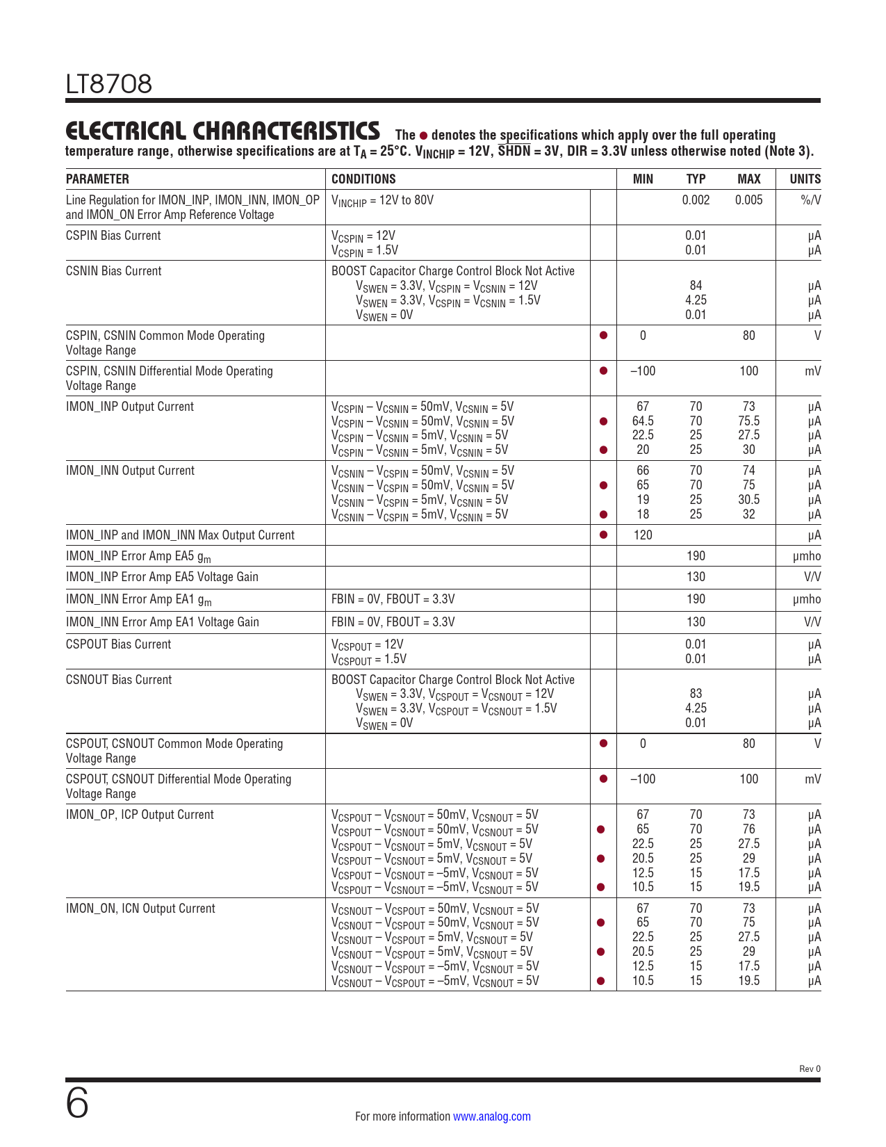
ELECTRICAL CHARACTERISTICS. The. denotes the specifications which apply over the full operating
Модельный ряд для этого даташита
Текстовая версия документа
LT8708
ELECTRICAL CHARACTERISTICS The
l
denotes the specifications which apply over the full operating temperature range, otherwise specifications are at TA = 25°C. VINCHIP = 12V, SHDN = 3V, DIR = 3.3V unless otherwise noted (Note 3). PARAMETER CONDITIONS MIN TYP MAX UNITS
Line Regulation for IMON_INP, IMON_INN, IMON_OP VINCHIP = 12V to 80V 0.002 0.005 %/V and IMON_ON Error Amp Reference Voltage CSPIN Bias Current VCSPIN = 12V 0.01 μA VCSPIN = 1.5V 0.01 μA CSNIN Bias Current BOOST Capacitor Charge Control Block Not Active VSWEN = 3.3V, VCSPIN = VCSNIN = 12V 84 μA VSWEN = 3.3V, VCSPIN = VCSNIN = 1.5V 4.25 μA VSWEN = 0V 0.01 μA CSPIN, CSNIN Common Mode Operating l 0 80 V Voltage Range CSPIN, CSNIN Differential Mode Operating l –100 100 mV Voltage Range IMON_INP Output Current VCSPIN – VCSNIN = 50mV, VCSNIN = 5V 67 70 73 μA VCSPIN – VCSNIN = 50mV, VCSNIN = 5V l 64.5 70 75.5 μA VCSPIN – VCSNIN = 5mV, VCSNIN = 5V 22.5 25 27.5 μA VCSPIN – VCSNIN = 5mV, VCSNIN = 5V l 20 25 30 μA IMON_INN Output Current VCSNIN – VCSPIN = 50mV, VCSNIN = 5V 66 70 74 μA VCSNIN – VCSPIN = 50mV, VCSNIN = 5V l 65 70 75 μA VCSNIN – VCSPIN = 5mV, VCSNIN = 5V 19 25 30.5 μA VCSNIN – VCSPIN = 5mV, VCSNIN = 5V l 18 25 32 μA IMON_INP and IMON_INN Max Output Current l 120 μA IMON_INP Error Amp EA5 gm 190 μmho IMON_INP Error Amp EA5 Voltage Gain 130 V/V IMON_INN Error Amp EA1 gm FBIN = 0V, FBOUT = 3.3V 190 μmho IMON_INN Error Amp EA1 Voltage Gain FBIN = 0V, FBOUT = 3.3V 130 V/V CSPOUT Bias Current VCSPOUT = 12V 0.01 μA VCSPOUT = 1.5V 0.01 μA CSNOUT Bias Current BOOST Capacitor Charge Control Block Not Active VSWEN = 3.3V, VCSPOUT = VCSNOUT = 12V 83 μA VSWEN = 3.3V, VCSPOUT = VCSNOUT = 1.5V 4.25 μA VSWEN = 0V 0.01 μA CSPOUT, CSNOUT Common Mode Operating l 0 80 V Voltage Range CSPOUT, CSNOUT Differential Mode Operating l –100 100 mV Voltage Range IMON_OP, ICP Output Current VCSPOUT – VCSNOUT = 50mV, VCSNOUT = 5V 67 70 73 μA VCSPOUT – VCSNOUT = 50mV, VCSNOUT = 5V l 65 70 76 μA VCSPOUT – VCSNOUT = 5mV, VCSNOUT = 5V 22.5 25 27.5 μA VCSPOUT – VCSNOUT = 5mV, VCSNOUT = 5V l 20.5 25 29 μA VCSPOUT – VCSNOUT = –5mV, VCSNOUT = 5V 12.5 15 17.5 μA VCSPOUT – VCSNOUT = –5mV, VCSNOUT = 5V l 10.5 15 19.5 μA IMON_ON, ICN Output Current VCSNOUT – VCSPOUT = 50mV, VCSNOUT = 5V 67 70 73 μA VCSNOUT – VCSPOUT = 50mV, VCSNOUT = 5V l 65 70 75 μA VCSNOUT – VCSPOUT = 5mV, VCSNOUT = 5V 22.5 25 27.5 μA VCSNOUT – VCSPOUT = 5mV, VCSNOUT = 5V l 20.5 25 29 μA VCSNOUT – VCSPOUT = –5mV, VCSNOUT = 5V 12.5 15 17.5 μA VCSNOUT – VCSPOUT = –5mV, VCSNOUT = 5V l 10.5 15 19.5 μA Rev 0 6 For more information www.analog.com Document Outline Features Applications Typical Application Description Absolute Maximum Ratings Order Information Pin Configuration Electrical Characteristics Typical Performance Characteristics Typical Performance Characteristics Pin Functions Block Diagram Operation Typographical Conventions Start-Up Start-Up: SHDN Pin Start-Up: SWEN Pin Start-Up: Soft-Start of Switching Regulator Control Overview Power Switch Control Switch Control: Buck Region (VIN >> VOUT) Switch Control: Buck-Boost (VIN ≅ VOUT) Switch Control: Boost Region (VIN << VOUT) Switch Control: Soft-Start Uni and Bidirectional Conduction Bidirectional Conduction: CCM Unidirectional Conduction: DCM Unidirectional Conduction: HCM Unidirectional Conduction: Burst Mode Error Amplifiers VOUT Regulation and Sensing VOUT: Regulation VOUT: Above Regulation VOUT: Below Regulation and Undervoltage VIN Regulation and Sensing VIN: Regulation VIN: Above Regulation and Overvoltage VIN: Below Regulation Current Monitoring and Limiting Monitoring and Limiting: IMON Pins Monitoring: ICP and ICN Pins INTVCC/EXTVCC/GATEVCC/LDO33 Power CLKOUT and Temperature Sensing Applications Information Verify the Power Flow Conditions Operating Frequency Selection Internal Oscillator SYNC Pin and Clock Synchronization CLKOUT Pin and Clock Synchronization Inductor Current Sensing and Slope Compensation RSENSE Selection and Maximum Current RSENSE Selection: Max RSENSE in the Boost Region RSENSE Selection: Max RSENSE in the Buck Region RSENSE Selection: Final RSENSE Value RSENSE Filtering Inductor (L) Selection L Selection: Load Current in Buck and Boost Regions L Selection: Subharmonic Oscillations L Selection: Maximum Current Rating Power MOSFET Selection CIN and COUT Selection Schottky Diode (D1, D2, D3, D4) Selection Topside MOSFET Driver Supply (CB1, DB1, CB2, DB2) Top Driver: Boost Cap Charge Control Block Top Driver: Boost Diodes DB1 and DB2 VINHIMON, VOUTLOMON and RVSOFF IIN and IOUT Current Monitoring and Limiting Loop Compensation INTVCC Regulators and EXTVCC Connection LDO33 Regulator Voltage Lockouts Junction Temperature Measurement Thermal Shutdown Efficiency Considerations Circuit Board Layout Checklist Hot Plugging Considerations Design Example Typical Applications Package Description Typical Application Related Parts

 Купить LT8708HLWE#WPBF на РадиоЛоцман.Цены — от 325 до 2 927 ₽


