Datasheet LTC4121, LTC4121-4.2 (Analog Devices) - 4
| Производитель | Analog Devices |
| Описание | 40V 400mA Synchronous Step-Down Battery Charger |
| Страниц / Страница | 30 / 4 — ELECTRICAL CHARACTERISTICS. The. denotes the specifications which apply … |
| Формат / Размер файла | PDF / 383 Кб |
| Язык документа | английский |
ELECTRICAL CHARACTERISTICS. The. denotes the specifications which apply over the specified operating
Модельный ряд для этого даташита
Текстовая версия документа
LTC4121/LTC4121-4.2
ELECTRICAL CHARACTERISTICS The
l
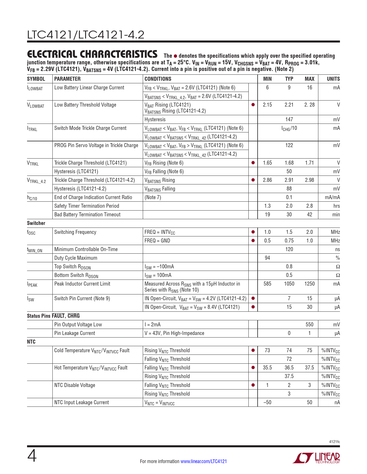
denotes the specifications which apply over the specified operating junction temperature range, otherwise specifications are at TA = 25°C. VIN = VRUN = 15V, VCHGSNS = VBAT = 4V, RPROG = 3.01k, VFB = 2.29V (LTC4121), VBATSNS = 4V (LTC4121-4.2). Current into a pin is positive out of a pin is negative. (Note 2) SYMBOL PARAMETER CONDITIONS MIN TYP MAX UNITS
ILOWBAT Low Battery Linear Charge Current VFB < VTRKL, VBAT = 2.6V (LTC4121) (Note 6) 6 9 16 mA VBATSNS < VTRKL_4.2, VBAT = 2.6V (LTC4121-4.2) VLOWBAT Low Battery Threshold Voltage VBAT Rising (LTC4121) l 2.15 2.21 2. 28 V VBATSNS Rising (LTC4121-4.2) Hysteresis 147 mV ITRKL Switch Mode Trickle Charge Current VLOWBAT < VBAT, VFB < VTRKL (LTC4121) (Note 6) ICHG/10 mA VLOWBAT < VBATSNS < VTRKL_42 (LTC4121-4.2) PROG Pin Servo Voltage in Trickle Charge VLOWBAT < VBAT, VFB > VTRKL (LTC4121) (Note 6) 122 mV VLOWBAT < VBATSNS < VTRKL_42 (LTC4121-4.2) VTRKL Trickle Charge Threshold (LTC4121) VFB Rising (Note 6) l 1.65 1.68 1.71 V Hysteresis (LTC4121) VFB Falling (Note 6) 50 mV VTRKL_4.2 Trickle Charge Threshold (LTC4121-4.2) VBATSNS Rising l 2.86 2.91 2.98 V Hysteresis (LTC4121-4.2) VBATSNS Falling 88 mV hC/10 End of Charge Indication Current Ratio (Note 7) 0.1 mA/mA Safety Timer Termination Period 1.3 2.0 2.8 hrs Bad Battery Termination Timeout 19 30 42 min
Switcher
fOSC Switching Frequency FREQ = INTVCC l 1.0 1.5 2.0 MHz FREQ = GND l 0.5 0.75 1.0 MHz tMIN_ON Minimum Controllable On-Time 120 ns Duty Cycle Maximum 94 % Top Switch RDSON ISW = –100mA 0.8 Ω Bottom Switch RDSON ISW = 100mA 0.5 Ω IPEAK Peak Inductor Current Limit Measured Across RSNS with a 15µH Inductor in 585 1050 1250 mA Series with RSNS (Note 10) ISW Switch Pin Current (Note 9) IN Open-Circuit, VBAT = VSW = 4.2V (LTC4121-4.2) l 7 15 µA IN Open-Circuit, VBAT = VSW = 8.4V (LTC4121) l 15 30 µA
Status Pins FAULT, CHRG
Pin Output Voltage Low I = 2mA 550 mV Pin Leakage Current V = 43V, Pin High-Impedance 0 1 µA
NTC
Cold Temperature VNTC/VINTVCC Fault Rising VNTC Threshold l 73 74 75 %INTVCC Falling VNTC Threshold 72 %INTVCC Hot Temperature VNTC/VINTVCC Fault Falling VNTC Threshold l 35.5 36.5 37.5 %INTVCC Rising VNTC Threshold 37.5 %INTVCC NTC Disable Voltage Falling VNTC Threshold l 1 2 3 %INTVCC Rising VNTC Threshold 3 %INTVCC NTC Input Leakage Current VNTC = VINTVCC –50 50 nA 4121fc 4 For more information www.linear.com/LTC4121 Document Outline Features Applications Typical Application Description Absolute Maximum Ratings Pin Configuration Order Information Electrical Characteristics Typical Performance Characteristics Pin Functions Block Diagram Operation Applications Information Applications Examples Package Description Typical Application Related Parts

 Купить LTC4121IUD-4.2#PBF на РадиоЛоцман.Цены — от 139 до 891 ₽

