Datasheet PCF8574, PCF8574A (NXP) - 5
| Производитель | NXP |
| Описание | Remote 8-bit I/O expander for I2C-bus with interrupt |
| Страниц / Страница | 33 / 5 — NXP Semiconductors. PCF8574; PCF8574A. Remote 8-bit I/O expander for … |
| Версия | 5.0 |
| Формат / Размер файла | PDF / 814 Кб |
| Язык документа | английский |
NXP Semiconductors. PCF8574; PCF8574A. Remote 8-bit I/O expander for I2C-bus with interrupt. 7. Functional. description

PCF8574; PCF8574A - Remote 8-bit I/O expander for I2C?bus with interrupt SOP 16-Pin |
| PCF8574T,118
NXP | 438 ₽ | |
| PCF8574T,118
NXP | по запросу | |
Модельный ряд для этого даташита
- PCF8574T PCF8574T,112 PCF8574T,118 PCF8574T/3,112 PCF8574T/3,118 PCF8574T/3,512 PCF8574T/3,518 PCF8574TS PCF8574TS/3,112 PCF8574TS/3,118 PCF8574TS/F3,112 PCF8574TS/F3,118 PCF8574TS/F3,512 PCF8574TS/F3,518
Текстовая версия документа
link to page 5 link to page 3 link to page 5
NXP Semiconductors PCF8574; PCF8574A Remote 8-bit I/O expander for I2C-bus with interrupt 7. Functional description
Refer to Figure 1 “Block diagram”.
7.1 Device address
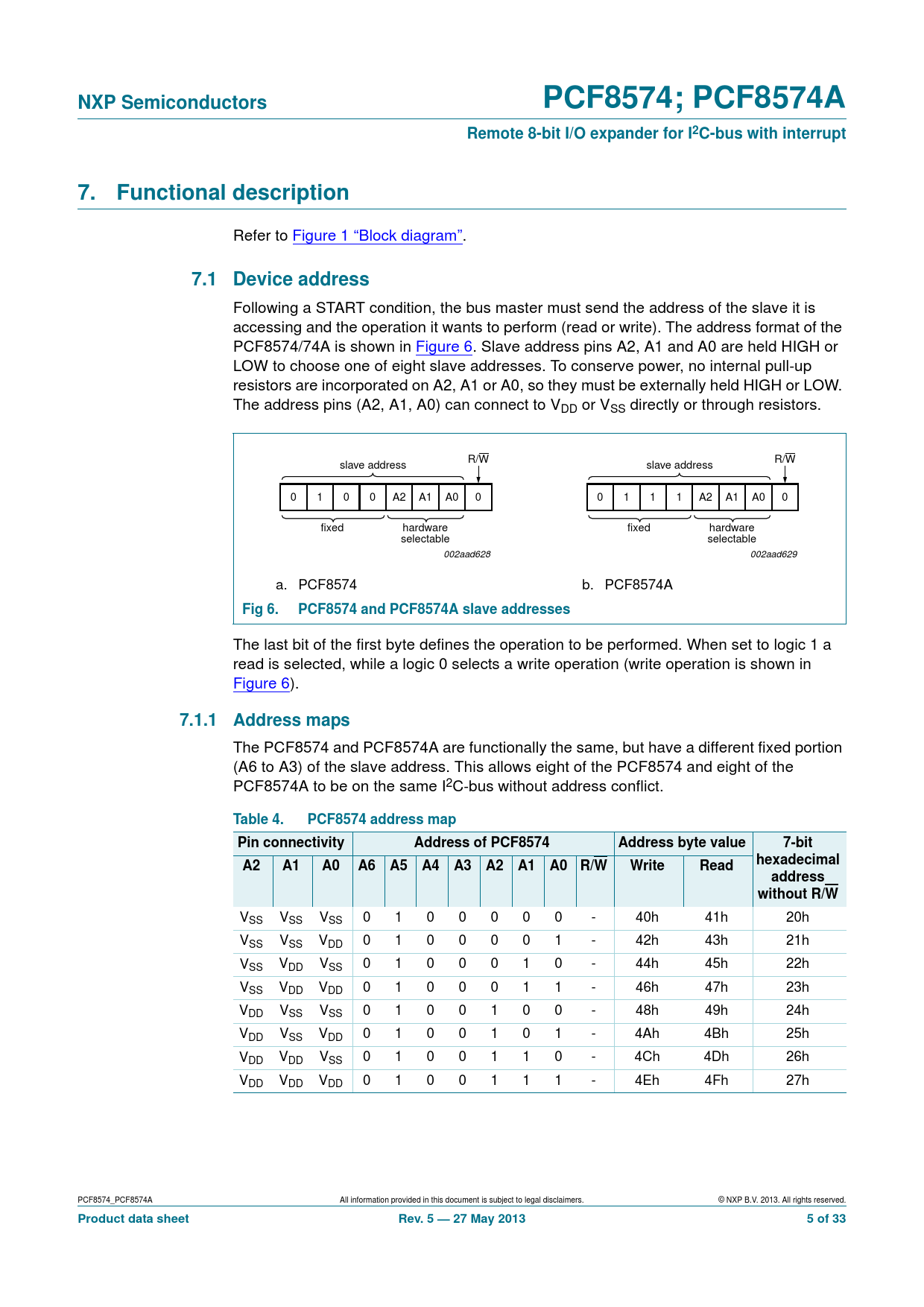
Following a START condition, the bus master must send the address of the slave it is accessing and the operation it wants to perform (read or write). The address format of the PCF8574/74A is shown in Figure 6. Slave address pins A2, A1 and A0 are held HIGH or LOW to choose one of eight slave addresses. To conserve power, no internal pull-up resistors are incorporated on A2, A1 or A0, so they must be externally held HIGH or LOW. The address pins (A2, A1, A0) can connect to VDD or VSS directly or through resistors. R/W R/W slave address slave address 0 1 0 0 A2 A1 A0 0 0 1 1 1 A2 A1 A0 0 fixed hardware fixed hardware selectable selectable 002aad628 002aad629 a. PCF8574 b. PCF8574A
Fig 6. PCF8574 and PCF8574A slave addresses
The last bit of the first byte defines the operation to be performed. When set to logic 1 a read is selected, while a logic 0 selects a write operation (write operation is shown in Figure 6).
7.1.1 Address maps
The PCF8574 and PCF8574A are functionally the same, but have a different fixed portion (A6 to A3) of the slave address. This allows eight of the PCF8574 and eight of the PCF8574A to be on the same I2C-bus without address conflict.
Table 4. PCF8574 address map Pin connectivity Address of PCF8574 Address byte value 7-bit hexadecimal A2 A1 A0 A6 A5 A4 A3 A2 A1 A0 R/W Write Read address without R/W
VSS VSS VSS 0 1 0 0 0 0 0 - 40h 41h 20h VSS VSS VDD 0 1 0 0 0 0 1 - 42h 43h 21h VSS VDD VSS 0 1 0 0 0 1 0 - 44h 45h 22h VSS VDD VDD 0 1 0 0 0 1 1 - 46h 47h 23h VDD VSS VSS 0 1 0 0 1 0 0 - 48h 49h 24h VDD VSS VDD 0 1 0 0 1 0 1 - 4Ah 4Bh 25h VDD VDD VSS 0 1 0 0 1 1 0 - 4Ch 4Dh 26h VDD VDD VDD 0 1 0 0 1 1 1 - 4Eh 4Fh 27h PCF8574_PCF8574A All information provided in this document is subject to legal disclaimers. © NXP B.V. 2013. All rights reserved.
Product data sheet Rev. 5 — 27 May 2013 5 of 33
Document Outline 1. General description 2. Features and benefits 3. Applications 4. Ordering information 4.1 Ordering options 5. Block diagram 6. Pinning information 6.1 Pinning 6.2 Pin description 7. Functional description 7.1 Device address 7.1.1 Address maps 8. I/O programming 8.1 Quasi-bidirectional I/Os 8.2 Writing to the port (Output mode) 8.3 Reading from a port (Input mode) 8.4 Power-on reset 8.5 Interrupt output (INT) 9. Characteristics of the I2C-bus 9.1 Bit transfer 9.1.1 START and STOP conditions 9.2 System configuration 9.3 Acknowledge 10. Application design-in information 10.1 Bidirectional I/O expander applications 10.2 How to read and write to I/O expander (example) 10.3 High current-drive load applications 10.4 Migration path 11. Limiting values 12. Thermal characteristics 13. Static characteristics 14. Dynamic characteristics 15. Package outline 16. Handling information 17. Soldering of SMD packages 17.1 Introduction to soldering 17.2 Wave and reflow soldering 17.3 Wave soldering 17.4 Reflow soldering 18. Soldering of through-hole mount packages 18.1 Introduction to soldering through-hole mount packages 18.2 Soldering by dipping or by solder wave 18.3 Manual soldering 18.4 Package related soldering information 19. Soldering: PCB footprints 20. Abbreviations 21. Revision history 22. Legal information 22.1 Data sheet status 22.2 Definitions 22.3 Disclaimers 22.4 Trademarks 23. Contact information 24. Contents