Datasheet LT1952, LT1952-1 (Analog Devices) - 4
| Производитель | Analog Devices |
| Описание | Single Switch Synchronous Forward Controller |
| Страниц / Страница | 28 / 4 — ELECTRICAL CHARACTERISTICS The. denotes the specifications which apply … |
| Формат / Размер файла | PDF / 371 Кб |
| Язык документа | английский |
ELECTRICAL CHARACTERISTICS The. denotes the specifications which apply over the specified operating

Модельный ряд для этого даташита
Текстовая версия документа
LT1952/LT1952-1
ELECTRICAL CHARACTERISTICS The
l
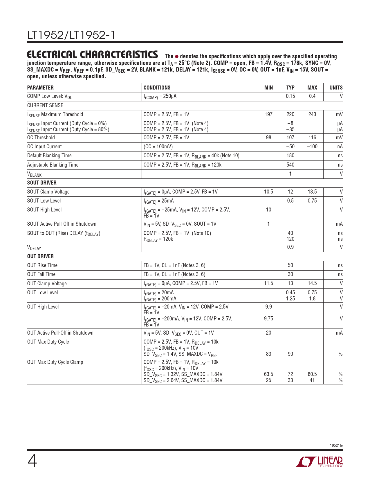
denotes the specifications which apply over the specified operating junction temperature range, otherwise specifications are at TA = 25°C (Note 2). COMP = open, FB = 1.4V, ROSC = 178k, SYNC = 0V, SS_MAXDC = VREF, VREF = 0.1µF, SD_VSEC = 2V, BLANK = 121k, DELAY = 121k, ISENSE = 0V, OC = 0V, OUT = 1nF, VIN = 15V, SOUT = open, unless otherwise specified. PARAMETER CONDITIONS MIN TYP MAX UNITS
COMP Low Level: VOL I(COMP) = 250µA 0.15 0.4 V CURRENT SENSE ISENSE Maximum Threshold COMP = 2.5V, FB = 1V 197 220 243 mV ISENSE Input Current (Duty Cycle = 0%) COMP = 2.5V, FB = 1V (Note 4) –8 µA ISENSE Input Current (Duty Cycle = 80%) COMP = 2.5V, FB = 1V (Note 4) –35 µA OC Threshold COMP = 2.5V, FB = 1V 98 107 116 mV OC Input Current (OC = 100mV) –50 –100 nA Default Blanking Time COMP = 2.5V, FB = 1V, RBLANK = 40k (Note 10) 180 ns Adjustable Blanking Time COMP = 2.5V, FB = 1V, RBLANK = 120k 540 ns VBLANK 1 V
SOUT DRIVER
SOUT Clamp Voltage I(GATE) = 0µA, COMP = 2.5V, FB = 1V 10.5 12 13.5 V SOUT Low Level I(GATE) = 25mA 0.5 0.75 V SOUT High Level I(GATE) = –25mA, VIN = 12V, COMP = 2.5V, 10 V FB = 1V SOUT Active Pull-Off in Shutdown VIN = 5V, SD_VSEC = 0V, SOUT = 1V 1 mA SOUT to OUT (Rise) DELAY (tDELAY) COMP = 2.5V, FB = 1V (Note 10) 40 ns RDELAY = 120k 120 ns VDELAY 0.9 V
OUT DRIVER
OUT Rise Time FB = 1V, CL = 1nF (Notes 3, 6) 50 ns OUT Fall Time FB = 1V, CL = 1nF (Notes 3, 6) 30 ns OUT Clamp Voltage I(GATE) = 0µA, COMP = 2.5V, FB = 1V 11.5 13 14.5 V OUT Low Level I(GATE) = 20mA 0.45 0.75 V I(GATE) = 200mA 1.25 1.8 V OUT High Level I(GATE) = –20mA, VIN = 12V, COMP = 2.5V, 9.9 V FB = 1V I(GATE) = –200mA, VIN = 12V, COMP = 2.5V, 9.75 V FB = 1V OUT Active Pull-Off in Shutdown VIN = 5V, SD_VSEC = 0V, OUT = 1V 20 mA OUT Max Duty Cycle COMP = 2.5V, FB = 1V, RDELAY = 10k (fOSC = 200kHz), VIN = 10V SD_VSEC = 1.4V, SS_MAXDC = VREF 83 90 % OUT Max Duty Cycle Clamp COMP = 2.5V, FB = 1V, RDELAY = 10k (fOSC = 200kHz), VIN = 10V SD_VSEC = 1.32V, SS_MAXDC = 1.84V 63.5 72 80.5 % SD_VSEC = 2.64V, SS_MAXDC = 1.84V 25 33 41 % 19521fe 4 Document Outline Features Applications Description Typical Application Absolute Maximum Ratings Pin Configuration Order Information Electrical Characteristics Typical Performance Characteristics Pin Functions Timing Diagram Block Diagram Operation Applications Information Typical Applications Revision History Package Description Related Parts

 Купить LT1952MPGN-1#TRPBF на РадиоЛоцман.Цены — от 420 до 1 243 ₽