Datasheet AD8452 (Analog Devices)
| Производитель | Analog Devices |
| Описание | Precision Integrated Analog Front End, Controller, and PWM for Battery Test and Formation Systems |
| Страниц / Страница | 35 / 1 — Precision Integrated Analog Front End, Controller,. and PWM for Battery … |
| Версия | A |
| Формат / Размер файла | PDF / 754 Кб |
| Язык документа | английский |
Precision Integrated Analog Front End, Controller,. and PWM for Battery Test and Formation Systems. Data Sheet. AD8452

Модельный ряд для этого даташита
Текстовая версия документа
Precision Integrated Analog Front End, Controller, and PWM for Battery Test and Formation Systems Data Sheet AD8452 FEATURES GENERAL DESCRIPTION CC and CV battery test and formation modes with
The AD8452 combines a precision analog front-end controller
transparent and automatic switchover, for systems of
and switch mode power supply (SMPS), pulse-width modulator
20 Ah or less
(PWM) driver into a single silicon platform for high volume
Precise measurement of voltage and current
battery testing and formation manufacturing. A precision
Independent feedback control blocks
instrumentation amplifier (in-amp) measures the battery charge/
Highly accurate, factory trimmed instrumentation and
discharge current to better than ±0.1% accuracy, while an equally
differential amplifiers
accurate difference amplifier measures the battery voltage.
In-amp for current sense gain: 66 V/V
Internal laser trimmed resistor networks establish the in-amp
Difference amplifier for voltage sense gain: 0.4 V/V
and difference amplifier gains (66 V/V and 0.4 V/V, respectively),
Stable over temperature: offset voltage drift <0.6 μV/°C
and stabilize the AD8452 performance across the rated
(maximum)
operating temperature range.
Gain drift: <3 ppm/°C (maximum)
Desired battery cycling current and voltage levels are established
Current sense CMRR: 120 dB minimum
by applying precise control voltages to the ISET and VSET
Popular SMPS control for charge/discharge
inputs. Actual charge and discharge current levels are sensed
High PWM linearity with internal ramp voltage
(usually by a high power, highly accurate shunt resistor) whose
50 kHz to 300 kHz user controlled switching frequency
value is carefully selected according to system parameters.
Synchronization output or input with adjustable phase shift
Switching between constant current (CC) and constant voltage
Programmable soft start
(CV) loop integration is instantaneous, automatic, and completely
APPLICATIONS
transparent to the observer. A logic high at the MODE input
Battery formation and testing
selects the charge or discharge mode (high for charge, low for
High efficiency battery test systems with recycle capability
discharge).
Battery conditioning (charging and discharging) systems
The AD8452 simplifies designs by providing excellent performance, functionality, and overall reliability in a space saving 48-lead, 7 mm × 7 mm × 1.4 mm LQFP package rated for operation at temperatures from −40°C to +85°C.
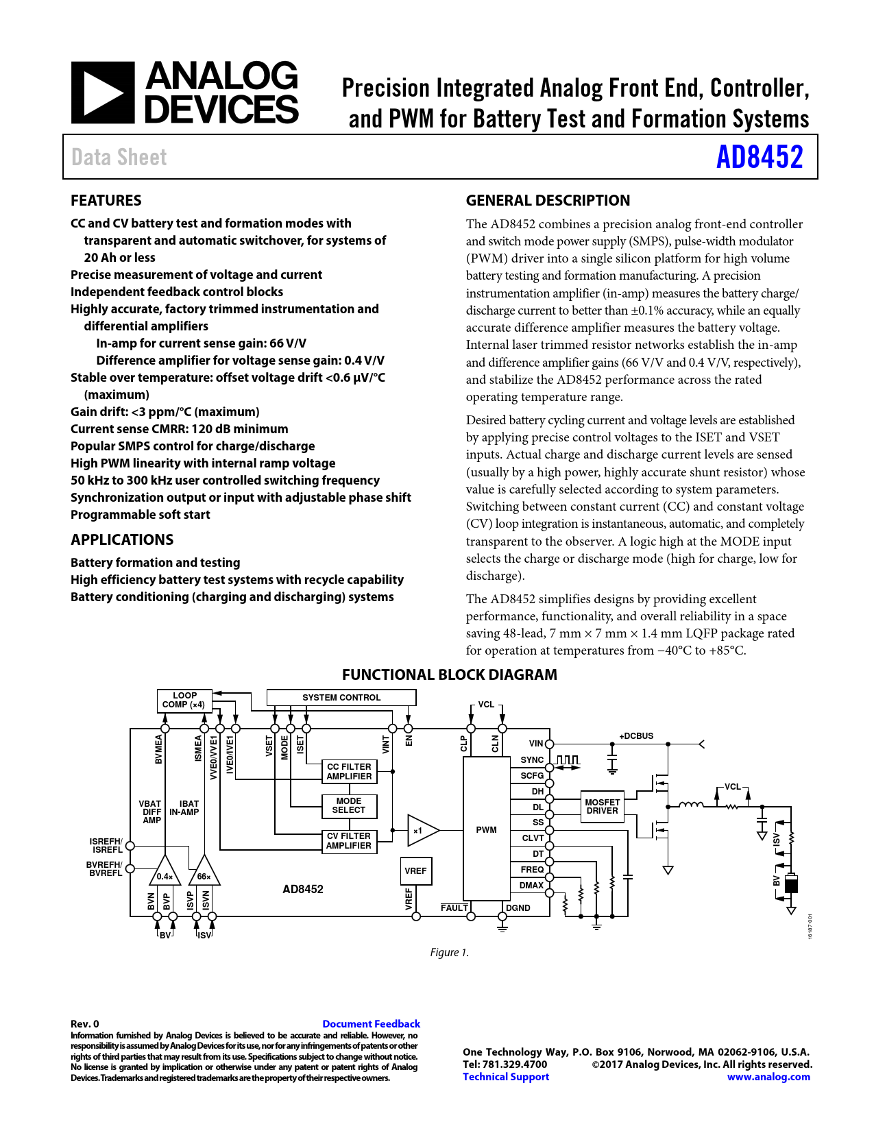
FUNCTIONAL BLOCK DIAGRAM LOOP SYSTEM CONTROL COMP (×4) VCL A E T T P N +DCBUS N EN VIN ME ISE /IVE1 VI CL CL VSET IS /VVE1 MOD BVMEA SYNC CC FILTER IVE0 VVE0 AMPLIFIER SCFG VCL DH VBAT IBAT MODE MOSFET DL DIFF IN-AMP SELECT DRIVER AMP SS ×1 PWM CV FILTER V ISREFH/ CLVT IS ISREFL AMPLIFIER DT BVREFH/ BVREFL VREF FREQ 0.4× 66× BV AD8452 DMAX N P EF BV ISVN ISVP BV VR FAULT DGND
1 00 7-
BV ISV
618 1 Figure 1.
Rev. 0 Document Feedback Information furnished by Analog Devices is believed to be accurate and reliable. However, no responsibility is assumed by Analog Devices for its use, nor for any infringements of patents or other rights of third parties that may result from its use. Specifications subject to change without notice. One Technology Way, P.O. Box 9106, Norwood, MA 02062-9106, U.S.A. No license is granted by implication or otherwise under any patent or patent rights of Analog Tel: 781.329.4700 ©2017 Analog Devices, Inc. All rights reserved. Devices. Trademarks and registered trademarks are the property of their respective owners. Technical Support www.analog.com
Document Outline Features Applications General Description Functional Block Diagram Table of Contents Revision History Specifications Analog Front-End and Controller Specifications Pulse-Width Modulator Specifications Digital Interface Specifications Power Supply Temperature Range Specifications Absolute Maximum Ratings Thermal Resistance ESD Caution Pin Configuration and Function Descriptions Typical Performance Characteristics In-Amp Characteristics Difference Amplifier Characteristics CC and CV Loop Filter Amplifiers and VSET Buffer (except where Noted) Reference Characteristics Pulse-Width Modulator Theory of Operation Introduction Instrumentation Amplifier (In-Amp) Reversing Polarity When Charging and Discharging In-Amp Offset Option Battery Reversal and Overvoltage Protection Difference Amplifier CC and CV Loop Filter Amplifiers Charging Lithium-Ion (Li-Ion) Cells Concepts of Constant Current (CC) and Constant Voltage (CV) Compensation Charge and Discharge Control Conditions to Charge and Discharge a Battery MODE Pin Input and Output Supply Pins Shutdown Undervoltage Lockout (UVLO) Soft Start PWM Drive Signals Peak Current Protection and Diode Emulation (Synchronous) Peak Current-Limit Detection Diode Emulation/Synchronous Mode Operation Frequency and Phase Control Internal Frequency Control External Frequency Control Operating Frequency Phase Shift Maximum Duty Cycle Fault Input Thermal Shutdown (TSD) Applications Information Analog Controller Functional Description Power Supply Connections Current Sense In-Amp Connections Current Sensors Optional Low-Pass Filter Voltage Sense Differential Amplifier Connections Battery Current and Voltage Control Inputs (ISET and VSET) Loop Filter Amplifiers Selecting Charge or Discharge Options Select RCL and RCLVT for the Peak Current Limit Setting the Operating Frequency and Programming the Synchonization Pin Select RFREQ for Standalone or Master Clock Selecting RFREQ for a Slave Device Programming the External Clock Phase Shift Programming the Dead Time Programming the Maximum Duty Cycle Selecting CSS Additional Information Outline Dimensions Ordering Guide

 Купить AD8452ASTZ-RL на РадиоЛоцман.Цены — от 883 до 28 463 ₽