Datasheet ADA4805-2-EP (Analog Devices)
| Производитель | Analog Devices |
| Описание | 0.2 µV/°C Offset Drift, 105 MHz Low Power, Low Noise, Rail-to-Rail Amplifier |
| Страниц / Страница | 9 / 1 — 0.4 µV/°C Offset Drift, 105 MHz Low Power,. Low Noise, Rail-to-Rail … |
| Формат / Размер файла | PDF / 249 Кб |
| Язык документа | английский |
0.4 µV/°C Offset Drift, 105 MHz Low Power,. Low Noise, Rail-to-Rail Amplifier. Enhanced Product. ADA4805-2-EP. FEATURES

Модельный ряд для этого даташита
Текстовая версия документа
link to page 1
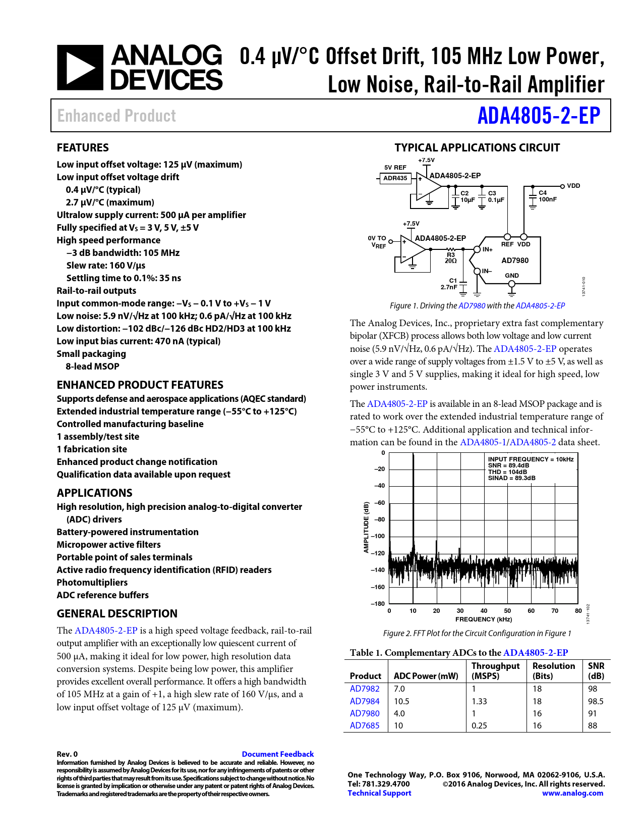
0.4 µV/°C Offset Drift, 105 MHz Low Power, Low Noise, Rail-to-Rail Amplifier Enhanced Product ADA4805-2-EP FEATURES TYPICAL APPLICATIONS CIRCUIT Low input offset voltage: 125 µV (maximum) +7.5V 5V REF Low input offset voltage drift ADA4805-2-EP ADR435 0.4 µV/°C (typical) VDD C2 C3 C4 2.7 µV/°C (maximum) 10µF 0.1µF 100nF Ultralow supply current: 500 µA per amplifier Fully specified at V +7.5V S = 3 V, 5 V, ±5 V High speed performance 0V TO ADA4805-2-EP V REF VDD REF −3 dB bandwidth: 105 MHz IN+ R3 Slew rate: 160 V/µs 20Ω AD7980 IN– Settling time to 0.1%: 35 ns GND C1
010
Rail-to-rail outputs 2.7nF
13741-
Input common-mode range: −VS − 0.1 V to +VS − 1 V
Figure 1. Driving the AD7980 with the ADA4805-2-EP
Low noise: 5.9 nV/√Hz at 100 kHz; 0.6 pA/√Hz at 100 kHz
The Analog Devices, Inc., proprietary extra fast complementary
Low distortion: −102 dBc/−126 dBc HD2/HD3 at 100 kHz Low input bias current: 470 nA (typical)
bipolar (XFCB) process allows both low voltage and low current
Small packaging
noise (5.9 nV/√Hz, 0.6 pA/√Hz). The ADA4805-2-EP operates
8-lead MSOP
over a wide range of supply voltages from ±1.5 V to ±5 V, as well as single 3 V and 5 V supplies, making it ideal for high speed, low
ENHANCED PRODUCT FEATURES
power instruments.
Supports defense and aerospace applications (AQEC standard)
The ADA4805-2-EP is available in an 8-lead MSOP package and is
Extended industrial temperature range (−55°C to +125°C)
rated to work over the extended industrial temperature range of
Controlled manufacturing baseline
−55°C to +125°C. Additional application and technical infor-
1 assembly/test site
mation can be found in the ADA4805-1/ADA4805-2 data sheet.
1 fabrication site 0 Enhanced product change notification INPUT FREQUENCY = 10kHz SNR = 89.4dB Qualification data available upon request –20 THD = 104dB SINAD = 89.3dB –40 APPLICATIONS High resolution, high precision analog-to-digital converter –60 B) d (ADC) drivers ( –80 Battery-powered instrumentation UDE IT L –100 Micropower active filters P AM Portable point of sales terminals –120 Active radio frequency identification (RFID) readers –140 Photomultipliers –160 ADC reference buffers –180 GENERAL DESCRIPTION 0 10 20 30 40 50 60 70 80
102
FREQUENCY (kHz)
13741- The ADA4805-2-EP is a high speed voltage feedback, rail-to-rail Figure 2. FFT Plot for the Circuit Configuration in Figure 1 output amplifier with an exceptional y low quiescent current of 500 µA, making it ideal for low power, high resolution data
Table 1. Complementary ADCs to the ADA4805-2-EP
conversion systems. Despite being low power, this amplifier
Throughput Resolution SNR
provides excellent overal performance. It offers a high bandwidth
Product ADC Power (mW) (MSPS) (Bits) (dB)
of 105 MHz at a gain of +1, a high slew rate of 160 V/µs, and a AD7982 7.0 1 18 98 low input offset voltage of 125 µV (maximum). AD7984 10.5 1.33 18 98.5 AD7980 4.0 1 16 91 AD7685 10 0.25 16 88
Rev. 0 Document Feedback Information furnished by Analog Devices is believed to be accurate and reliable. However, no responsibility is assumed by Analog Devices for its use, nor for any infringements of patents or other rights of third parties that may result from its use. Specifications subject to change without notice. No One Technology Way, P.O. Box 9106, Norwood, MA 02062-9106, U.S.A. license is granted by implication or otherwise under any patent or patent rights of Analog Devices. Tel: 781.329.4700 ©2016 Analog Devices, Inc. All rights reserved. Trademarks and registered trademarks are the property of their respective owners. Technical Support www.analog.com
Document Outline FEATURES ENHANCED PRODUCT FEATURES APPLICATIONS GENERAL DESCRIPTION TYPICAL APPLICATIONS CIRCUIT TABLE OF CONTENTS REVISION HISTORY SPECIFICATIONS ±5 V SUPPLY 5 V SUPPLY 3 V SUPPLY ABSOLUTE MAXIMUM RATINGS THERMAL RESISTANCE MAXIMUM POWER DISSIPATION ESD CAUTION PIN CONFIGURATION AND FUNCTION DESCRIPTIONS TYPICAL PERFORMANCE CHARACTERISTICS OUTLINE DIMENSIONS ORDERING GUIDE
 Купить ADA4805-2ARMZ-R7 на РадиоЛоцман.Цены — от 102 до 31 574 ₽