Datasheet AD9260 (Analog Devices)
| Производитель | Analog Devices |
| Описание | 16-Bit High Speed Oversampled A/D Converter |
| Страниц / Страница | 45 / 1 — High Speed Oversampling CMOS ADC with. 16-Bit Resolution at a 2.5 MHz … |
| Версия | C |
| Формат / Размер файла | PDF / 1.1 Мб |
| Язык документа | английский |
High Speed Oversampling CMOS ADC with. 16-Bit Resolution at a 2.5 MHz Output Word Rate. AD9260. FEATURES

10 предложений от 10 поставщиков Микросхема Преобразователь AD, ADC Single Pipelined 2.5MSPS 16Bit Parallel 44Pin MQFP T/R |
| AD9260ASZRL
Analog Devices | 8 553 ₽ | |
| AD9260ASZRL
Analog Devices | 9 633 ₽ | |
| AD9260ASZRL
Analog Devices | 11 554 ₽ | |
| AD9260ASZRL
Analog Devices | по запросу | |
Модельный ряд для этого даташита
Текстовая версия документа
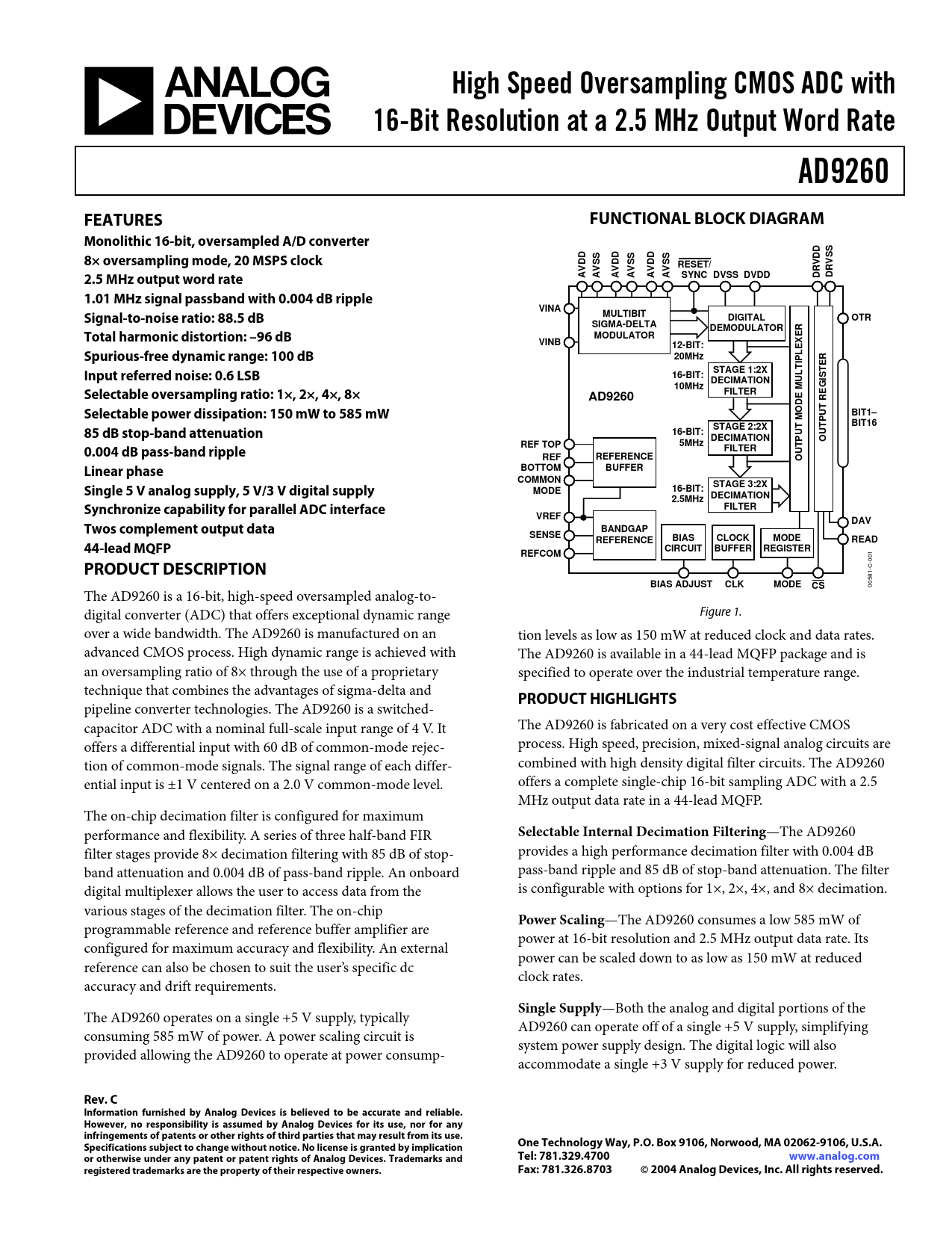
High Speed Oversampling CMOS ADC with 16-Bit Resolution at a 2.5 MHz Output Word Rate AD9260 FEATURES FUNCTIONAL BLOCK DIAGRAM Monolithic 16-bit, oversampled A/D converter 8× oversampling mode, 20 MSPS clock DD DD DD DD VSS VSS RESET/ VSS VSS R 2.5 MHz output word rate AV A AV A AV A SYNC DVSS DVDD DRV D 1.01 MHz signal passband with 0.004 dB ripple VINA Signal-to-noise ratio: 88.5 dB MULTIBIT DIGITAL OTR SIGMA-DELTA DEMODULATOR Total harmonic distortion: –96 dB MODULATOR VINB 12-BIT: Spurious-free dynamic range: 100 dB 20MHz R E STAGE 1:2X T Input referred noise: 0.6 LSB LTIPLEXER 16-BIT: DECIMATION U 10MHz GIS Selectable oversampling ratio: 1×, 2×, 4×, 8× FILTER M E AD9260 D Selectable power dissipation: 150 mW to 585 mW O UT RE BIT1– M STAGE 2:2X T BIT16 85 dB stop-band attenuation 16-BIT: DECIMATION OUTP REF TOP 5MHz TPU 0.004 dB pass-band ripple FILTER REF REFERENCE OU Linear phase BOTTOM BUFFER COMMON STAGE 3:2X Single 5 V analog supply, 5 V/3 V digital supply 16-BIT: MODE DECIMATION 2.5MHz Synchronize capability for parallel ADC interface FILTER VREF DAV Twos complement output data BANDGAP SENSE CLOCK MODE REFERENCE BIAS READ 44-lead MQFP CIRCUIT BUFFER REGISTER REFCOM PRODUCT DESCRIPTION BIAS ADJUST CLK MODE CS
00581-C-001 The AD9260 is a 16-bit, high-speed oversampled analog-to- digital converter (ADC) that offers exceptional dynamic range Figure 1. over a wide bandwidth. The AD9260 is manufactured on an tion levels as low as 150 mW at reduced clock and data rates. advanced CMOS process. High dynamic range is achieved with The AD9260 is available in a 44-lead MQFP package and is an oversampling ratio of 8× through the use of a proprietary specified to operate over the industrial temperature range. technique that combines the advantages of sigma-delta and
PRODUCT HIGHLIGHTS
pipeline converter technologies. The AD9260 is a switched- capacitor ADC with a nominal full-scale input range of 4 V. It The AD9260 is fabricated on a very cost effective CMOS offers a differential input with 60 dB of common-mode rejec- process. High speed, precision, mixed-signal analog circuits are tion of common-mode signals. The signal range of each differ- combined with high density digital filter circuits. The AD9260 ential input is ±1 V centered on a 2.0 V common-mode level. offers a complete single-chip 16-bit sampling ADC with a 2.5 MHz output data rate in a 44-lead MQFP. The on-chip decimation filter is configured for maximum performance and flexibility. A series of three half-band FIR
Selectable Internal Decimation Filtering
—The AD9260 filter stages provide 8× decimation filtering with 85 dB of stop- provides a high performance decimation filter with 0.004 dB band attenuation and 0.004 dB of pass-band ripple. An onboard pass-band ripple and 85 dB of stop-band attenuation. The filter digital multiplexer allows the user to access data from the is configurable with options for 1×, 2×, 4×, and 8× decimation. various stages of the decimation filter. The on-chip
Power Scaling
—The AD9260 consumes a low 585 mW of programmable reference and reference buffer amplifier are power at 16-bit resolution and 2.5 MHz output data rate. Its configured for maximum accuracy and flexibility. An external power can be scaled down to as low as 150 mW at reduced reference can also be chosen to suit the user’s specific dc clock rates. accuracy and drift requirements.
Single Supply
—Both the analog and digital portions of the The AD9260 operates on a single +5 V supply, typically AD9260 can operate off of a single +5 V supply, simplifying consuming 585 mW of power. A power scaling circuit is system power supply design. The digital logic will also provided allowing the AD9260 to operate at power consump- accommodate a single +3 V supply for reduced power.
Rev. C Information furnished by Analog Devices is believed to be accurate and reliable. However, no responsibility is assumed by Analog Devices for its use, nor for any infringements of patents or other rights of third parties that may result from its use. Specifications subject to change without notice. No license is granted by implication One Technology Way, P.O. Box 9106, Norwood, MA 02062-9106, U.S.A. or otherwise under any patent or patent rights of Analog Devices. Trademarks and Tel: 781.329.4700 www.analog.com registered trademarks are the property of their respective owners. Fax: 781.326.8703 © 2004 Analog Devices, Inc. All rights reserved.
Document Outline FEATURES PRODUCT DESCRIPTION FUNCTIONAL BLOCK DIAGRAM PRODUCT HIGHLIGHTS SPECIFICATIONS CLOCK INPUT FREQUENCY RANGE DC SPECIFICATIONS AC SPECIFICATIONS DIGITAL FILTER CHARACTERISTICS DIGITAL FILTER CHARACTERISTICS DIGITAL SPECIFICATIONS SWITCHING SPECIFICATIONS ABSOLUTE MAXIMUM RATINGS THERMAL CHARACTERISTICS ESD CAUTION TERMINOLOGY PIN CONFIGURATION AND FUNCTION DESCRIPTIONS TYPICAL PERFORMANCE CHARACTERISTICS TYPICAL AC CHARACTERIZATION CURVES VS. DECIMATION MODE TYPICAL AC CHARACTERIZATION CURVES FOR 8× MODE TYPICAL AC CHARACTERIZATION CURVES FOR 4× MODE TYPICAL AC CHARACTERIZATION CURVES FOR 2× MODE TYPICAL AC CHARACTERIZATION CURVES FOR 1× MODE TYPICAL AC CHARACTERIZATION CURVES ADDITIONAL AC CHARACTERIZATION CURVES THEORY OF OPERATION ANALOG INPUT AND REFERENCE OVERVIEW INPUT SPAN INPUT COMPLIANCE RANGE ANALOG INPUT OPERATION DRIVING THE INPUT Transient Response Input Driver Considerations Single-Ended-to-Differential Op Amp Driver Common-Mode Level REFERENCE OPERATION DIGITAL INPUTS AND OUTPUTS DIGITAL OUTPUTS CS and Read Pins DAV Pin RESET Pin OTR Pin MODE OPERATION BIAS PIN OPERATION POWER DISSIPATION CONSIDERATIONS DIGITAL OUTPUT DRIVER CONSIDERATIONS (DRVDD) Clock Input and Considerations GROUNDING AND DECOUPLING Analog and Digital Grounding Analog and Digital Supply Decoupling EVALUATION BOARD GENERAL DESCRIPTION FEATURES AND USER CONTROLS Jumper Controlled Mode/OSR Selection Selectable Power Bias Data Interfacing Controls Buffered Output Data Jumper Controlled Reference Source Flexible DC or AC Coupled External Clock Inputs Flexible Input Signal Configuration Circuitry Selecting Single or Dual Signal Input Selectable Input Signal Common-Mode Level Source SHIPMENT CONFIGURATION QUICK SETUP APPLICATION INFORMATION OUTLINE DIMENSIONS ORDERING GUIDE
 Купить AD9260ASZRL на РадиоЛоцман.Цены — от 727 до 12 157 ₽