Datasheet AD7792, AD7793 (Analog Devices)
| Производитель | Analog Devices |
| Описание | 3-Channel, Low Noise, Low Power, 24-Bit Sigma Delta ADC with On-Chip In-Amp and Reference |
| Страниц / Страница | 32 / 1 — 3-Channel, Low Noise, Low Power, 16-/24-Bit. ∑-Δ. ADC with On-Chip In-Amp … |
| Версия | B |
| Формат / Размер файла | PDF / 464 Кб |
| Язык документа | английский |
3-Channel, Low Noise, Low Power, 16-/24-Bit. ∑-Δ. ADC with On-Chip In-Amp and Reference. AD7792/AD7793. FEATURES

69 предложений от 29 поставщиков АЦП.Тип: Аналогово-цифровой преобразователь (АЦП) серии AD7792Вес брутто: 0.44Транспортная упаковка: размер/кол-во: 62*40*43/240Мощность: рассеиваемая - 2,5 мВтХарактеристика: INL - интегральная нелинейность ± 15... |
| AD7792BRUZ-REEL
Analog Devices | 327 ₽ | |
| AD7792BRUZ-REEL
Analog Devices | от 527 ₽ | |
| AD7792BRUZ-REEL
Analog Devices | 1 019 ₽ | |
| AD7792BRUZ-REEL
Analog Devices | по запросу | |
Модельный ряд для этого даташита
Текстовая версия документа
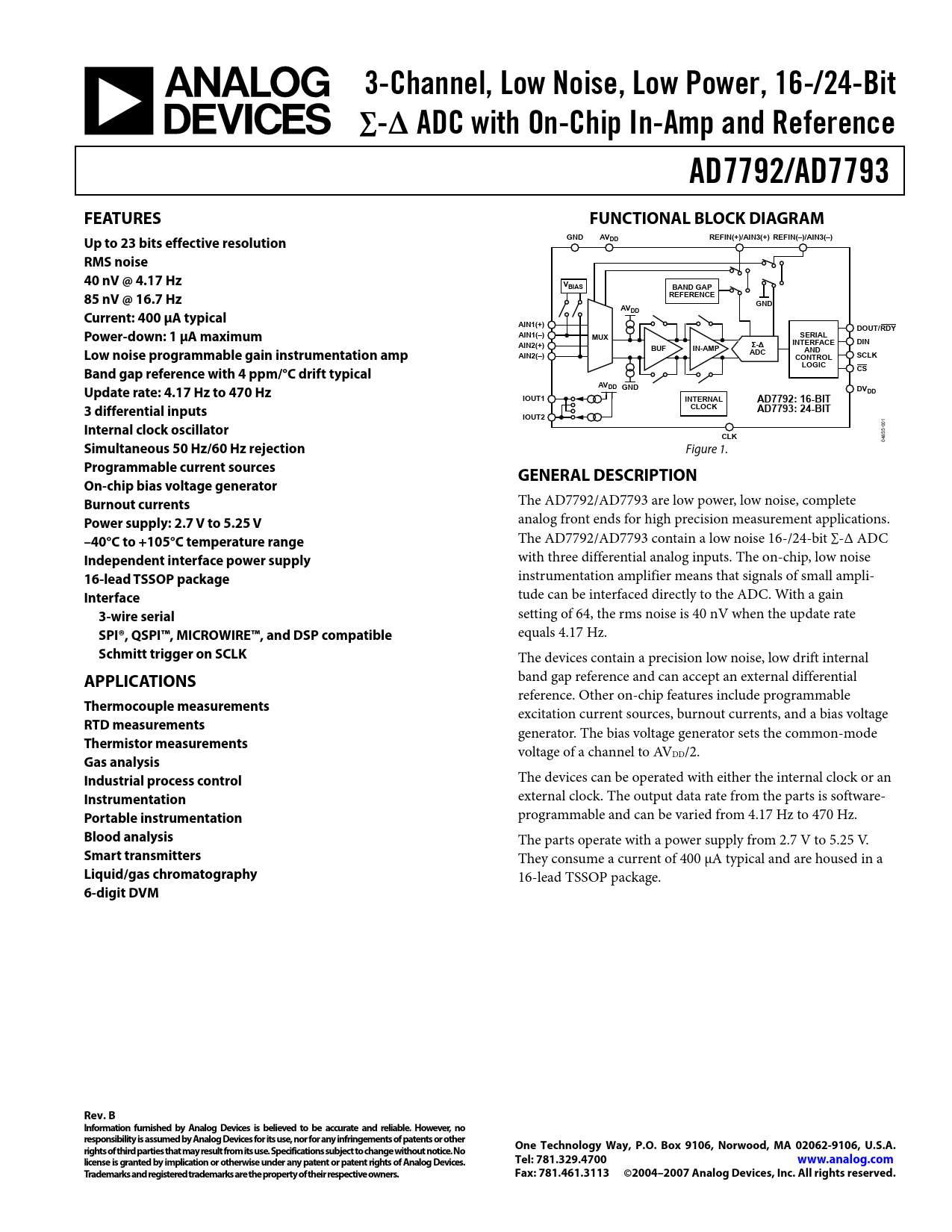
3-Channel, Low Noise, Low Power, 16-/24-Bit ∑-Δ ADC with On-Chip In-Amp and Reference AD7792/AD7793 FEATURES FUNCTIONAL BLOCK DIAGRAM GND AV REFIN(+)/AIN3(+) Up to 23 bits effective resolution DD REFIN(–)/AIN3(–) RMS noise 40 nV @ 4.17 Hz VBIAS BAND GAP 85 nV @ 16.7 Hz REFERENCE GND AVDD Current: 400 μA typical AIN1(+) DOUT/RDY Power-down: 1 μA maximum AIN1(–) SERIAL MUX INTERFACE DIN AIN2(+) Σ-Δ BUF IN-AMP AND Low noise programmable gain instrumentation amp ADC AIN2(–) SCLK CONTROL LOGIC CS Band gap reference with 4 ppm/°C drift typical AVDD GND Update rate: 4.17 Hz to 470 Hz DVDD IOUT1 INTERNAL AD7792: 16-BIT 3 differential inputs CLOCK AD7793: 24-BIT IOUT2
1
Internal clock oscillator
00 5-
CLK
0485
Simultaneous 50 Hz/60 Hz rejection
Figure 1.
Programmable current sources GENERAL DESCRIPTION On-chip bias voltage generator Burnout currents
The AD7792/AD7793 are low power, low noise, complete
Power supply: 2.7 V to 5.25 V
analog front ends for high precision measurement applications.
–40°C to +105°C temperature range
The AD7792/AD7793 contain a low noise 16-/24-bit ∑-Δ ADC
Independent interface power supply
with three differential analog inputs. The on-chip, low noise
16-lead TSSOP package
instrumentation amplifier means that signals of small ampli-
Interface
tude can be interfaced directly to the ADC. With a gain
3-wire serial
setting of 64, the rms noise is 40 nV when the update rate
SPI®, QSPI™, MICROWIRE™, and DSP compatible
equals 4.17 Hz.
Schmitt trigger on SCLK
The devices contain a precision low noise, low drift internal
APPLICATIONS
band gap reference and can accept an external differential reference. Other on-chip features include programmable
Thermocouple measurements
excitation current sources, burnout currents, and a bias voltage
RTD measurements
generator. The bias voltage generator sets the common-mode
Thermistor measurements
voltage of a channel to AVDD/2.
Gas analysis Industrial process control
The devices can be operated with either the internal clock or an
Instrumentation
external clock. The output data rate from the parts is software-
Portable instrumentation
programmable and can be varied from 4.17 Hz to 470 Hz.
Blood analysis
The parts operate with a power supply from 2.7 V to 5.25 V.
Smart transmitters
They consume a current of 400 μA typical and are housed in a
Liquid/gas chromatography
16-lead TSSOP package.
6-digit DVM Rev. B Information furnished by Analog Devices is believed to be accurate and reliable. However, no responsibility is assumed by Analog Devices for its use, nor for any infringements of patents or other One Technology Way, P.O. Box 9106, Norwood, MA 02062-9106, U.S.A. rights of third parties that may result from its use. Specifications subject to change without notice. No license is granted by implication or otherwise under any patent or patent rights of Analog Devices. Tel: 781.329.4700 www.analog.com Trademarks and registered trademarks are the property of their respective owners. Fax: 781.461.3113 ©2004–2007 Analog Devices, Inc. All rights reserved.
Document Outline FEATURES APPLICATIONS FUNCTIONAL BLOCK DIAGRAM GENERAL DESCRIPTION TABLE OF CONTENTS REVISION HISTORY SPECIFICATIONS TIMING CHARACTERISTICS TIMING DIAGRAMS ABSOLUTE MAXIMUM RATINGS ESD CAUTION PIN CONFIGURATION AND FUNCTION DESCRIPTIONS OUTPUT NOISE AND RESOLUTION SPECIFICATIONS EXTERNAL REFERENCE INTERNAL REFERENCE TYPICAL PERFORMANCE CHARACTERISTICS ON-CHIP REGISTERS COMMUNICATIONS REGISTER RS2, RS1, RS0 = 0, 0, 0 STATUS REGISTER RS2, RS1, RS0 = 0, 0, 0; Power-On/Reset = 0x80 (AD7792)/0x88 (AD7793) MODE REGISTER RS2, RS1, RS0 = 0, 0, 1; Power-On/Reset = 0x000A CONFIGURATION REGISTER RS2, RS1, RS0 = 0, 1, 0; Power-On/Reset = 0x0710 DATA REGISTER RS2, RS1, RS0 = 0, 1, 1; Power-On/Reset = 0x0000(00) ID REGISTER RS2, RS1, RS0 = 1, 0, 0; Power-On/Reset = 0xXA (AD7792)/0xXB (AD7793) IO REGISTER RS2, RS1, RS0 = 1, 0, 1; Power-On/Reset = 0x00 OFFSET REGISTER RS2, RS1, RS0 = 1, 1, 0; Power-On/Reset = 0x8000 (AD7792)/0x800000 (AD7793) FULL-SCALE REGISTER RS2, RS1, RS0 = 1, 1, 1; Power-On/Reset = 0x5XXX (AD7792)/0x5XXX00 (AD7793) ADC CIRCUIT INFORMATION OVERVIEW DIGITAL INTERFACE Single Conversion Mode Continuous Conversion Mode Continuous Read CIRCUIT DESCRIPTION ANALOG INPUT CHANNEL INSTRUMENTATION AMPLIFIER BIPOLAR/UNIPOLAR CONFIGURATION DATA OUTPUT CODING BURNOUT CURRENTS EXCITATION CURRENTS BIAS VOLTAGE GENERATOR REFERENCE RESET AVDD MONITOR CALIBRATION GROUNDING AND LAYOUT APPLICATIONS INFORMATION TEMPERATURE MEASUREMENT USING A THERMOCOUPLE TEMPERATURE MEASUREMENT USING AN RTD OUTLINE DIMENSIONS ORDERING GUIDE
 Купить AD7792BRUZ-REEL на РадиоЛоцман.Цены — от 205 до 22 888 ₽