Datasheet AD9233 (Analog Devices)
| Производитель | Analog Devices |
| Описание | 12-Bit, 80 MSPS/105 MSPS/125 MSPS, 1.8 V Analog-to-Digital Converter |
| Страниц / Страница | 45 / 1 — 12-Bit, 80 MSPS/105 MSPS/125 MSPS,. 1.8 V Analog-to-Digital Converter. … |
| Версия | A |
| Формат / Размер файла | PDF / 1.0 Мб |
| Язык документа | английский |
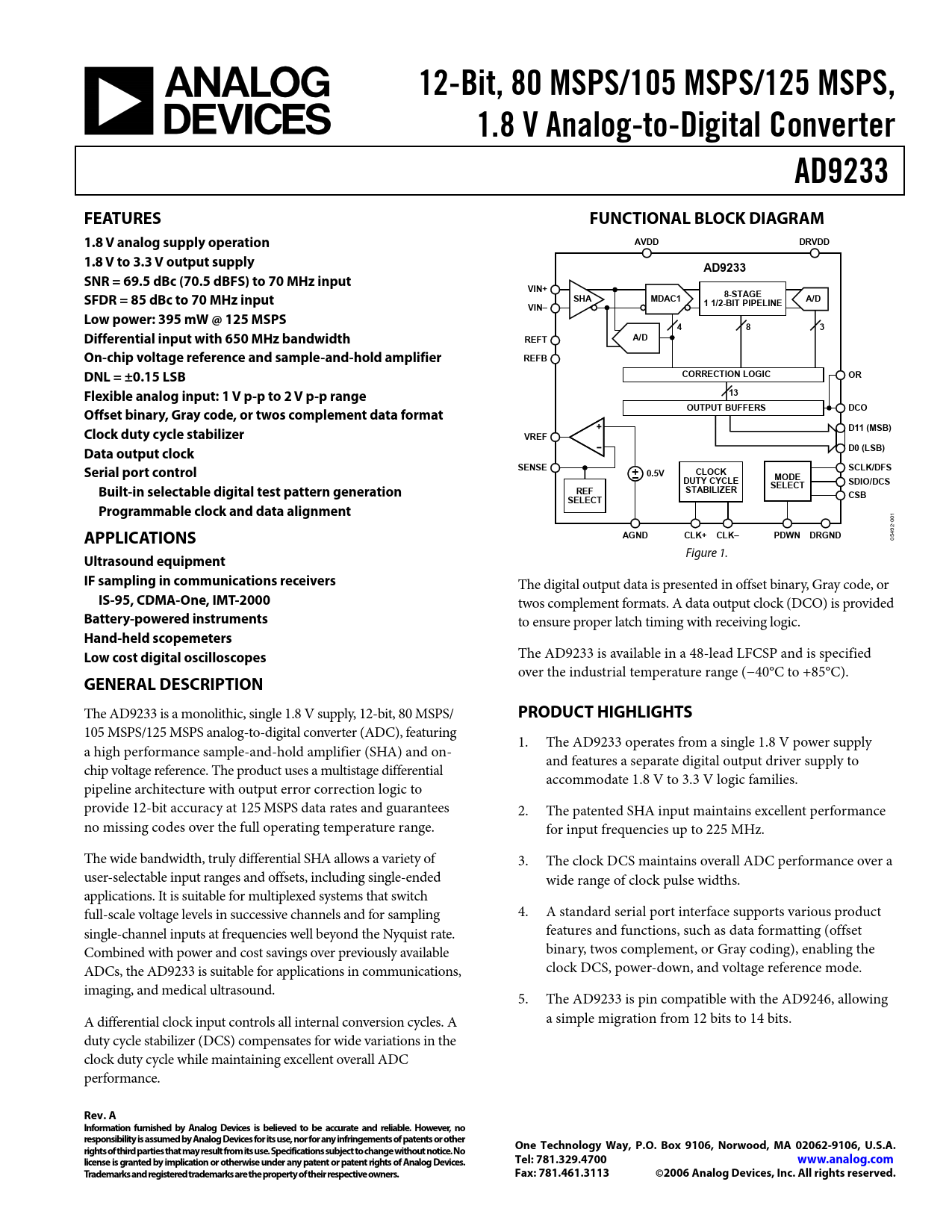
12-Bit, 80 MSPS/105 MSPS/125 MSPS,. 1.8 V Analog-to-Digital Converter. AD9233. FEATURES. FUNCTIONAL BLOCK DIAGRAM

Модельный ряд для этого даташита
Текстовая версия документа
12-Bit, 80 MSPS/105 MSPS/125 MSPS, 1.8 V Analog-to-Digital Converter AD9233 FEATURES FUNCTIONAL BLOCK DIAGRAM 1.8 V analog supply operation AVDD DRVDD 1.8 V to 3.3 V output supply AD9233 SNR = 69.5 dBc (70.5 dBFS) to 70 MHz input VIN+ 8-STAGE SFDR = 85 dBc to 70 MHz input SHA MDAC1 A/D 1 1/2-BIT PIPELINE VIN– Low power: 395 mW @ 125 MSPS 4 8 3 Differential input with 650 MHz bandwidth REFT A/D On-chip voltage reference and sample-and-hold amplifier REFB DNL = ±0.15 LSB CORRECTION LOGIC OR Flexible analog input: 1 V p-p to 2 V p-p range 13 OUTPUT BUFFERS DCO Offset binary, Gray code, or twos complement data format D11 (MSB) Clock duty cycle stabilizer VREF D0 (LSB) Data output clock Serial port control SENSE SCLK/DFS 0.5V CLOCK DUTY CYCLE MODE SELECT SDIO/DCS Built-in selectable digital test pattern generation REF STABILIZER CSB SELECT Programmable clock and data alignment
001
APPLICATIONS AGND CLK+ CLK– PDWN DRGND
05492- Figure 1.
Ultrasound equipment IF sampling in communications receivers
The digital output data is presented in offset binary, Gray code, or
IS-95, CDMA-One, IMT-2000
twos complement formats. A data output clock (DCO) is provided
Battery-powered instruments
to ensure proper latch timing with receiving logic.
Hand-held scopemeters Low cost digital oscilloscopes
The AD9233 is available in a 48-lead LFCSP and is specified over the industrial temperature range (−40°C to +85°C).
GENERAL DESCRIPTION
The AD9233 is a monolithic, single 1.8 V supply, 12-bit, 80 MSPS/
PRODUCT HIGHLIGHTS
105 MSPS/125 MSPS analog-to-digital converter (ADC), featuring 1. The AD9233 operates from a single 1.8 V power supply a high performance sample-and-hold amplifier (SHA) and on- and features a separate digital output driver supply to chip voltage reference. The product uses a multistage differential accommodate 1.8 V to 3.3 V logic families. pipeline architecture with output error correction logic to provide 12-bit accuracy at 125 MSPS data rates and guarantees 2. The patented SHA input maintains excellent performance no missing codes over the full operating temperature range. for input frequencies up to 225 MHz. The wide bandwidth, truly differential SHA allows a variety of 3. The clock DCS maintains overall ADC performance over a user-selectable input ranges and offsets, including single-ended wide range of clock pulse widths. applications. It is suitable for multiplexed systems that switch full-scale voltage levels in successive channels and for sampling 4. A standard serial port interface supports various product single-channel inputs at frequencies well beyond the Nyquist rate. features and functions, such as data formatting (offset Combined with power and cost savings over previously available binary, twos complement, or Gray coding), enabling the ADCs, the AD9233 is suitable for applications in communications, clock DCS, power-down, and voltage reference mode. imaging, and medical ultrasound. 5. The AD9233 is pin compatible with the AD9246, allowing A differential clock input controls all internal conversion cycles. A a simple migration from 12 bits to 14 bits. duty cycle stabilizer (DCS) compensates for wide variations in the clock duty cycle while maintaining excellent overall ADC performance.
Rev. A Information furnished by Analog Devices is believed to be accurate and reliable. However, no responsibility is assumed by Analog Devices for its use, nor for any infringements of patents or other One Technology Way, P.O. Box 9106, Norwood, MA 02062-9106, U.S.A. rights of third parties that may result from its use. Specifications subject to change without notice. No license is granted by implication or otherwise under any patent or patent rights of Analog Devices. Tel: 781.329.4700 www.analog.com Trademarks and registered trademarks are the property of their respective owners. Fax: 781.461.3113 ©2006 Analog Devices, Inc. All rights reserved.
Document Outline FEATURES APPLICATIONS GENERAL DESCRIPTION FUNCTIONAL BLOCK DIAGRAM PRODUCT HIGHLIGHTS TABLE OF CONTENTS REVISION HISTORY SPECIFICATIONS DC SPECIFICATIONS AC SPECIFICATIONS DIGITAL SPECIFICATIONS SWITCHING SPECIFICATIONS TIMING DIAGRAM ABSOLUTE MAXIMUM RATINGS THERMAL RESISTANCE ESD CAUTION PIN CONFIGURATION AND FUNCTION DESCRIPTIONS EQUIVALENT CIRCUITS TYPICAL PERFORMANCE CHARACTERISTICS THEORY OF OPERATION ANALOG INPUT CONSIDERATIONS Input Common Mode Differential Input Configurations Single-Ended Input Configuration VOLTAGE REFERENCE Internal Reference Connection External Reference Operation CLOCK INPUT CONSIDERATIONS Clock Input Options Clock Duty Cycle JITTER CONSIDERATIONS POWER DISSIPATION AND STANDBY MODE Power-Down Mode Standby Mode DIGITAL OUTPUTS Out-of-Range (OR) Condition Digital Output Enable Function (OEB) TIMING Data Clock Output (DCO) SERIAL PORT INTERFACE (SPI) CONFIGURATION USING THE SPI HARDWARE INTERFACE CONFIGURATION WITHOUT THE SPI MEMORY MAP READING THE MEMORY MAP TABLE Open Locations Default Values Logic Levels SPI-Accessible Features LAYOUT CONSIDERATIONS POWER AND GROUND RECOMMENDATIONS Exposed Paddle Thermal Heat Slug Recommendations CML RBIAS REFERENCE DECOUPLING EVALUATION BOARD POWER SUPPLIES INPUT SIGNALS OUTPUT SIGNALS DEFAULT OPERATION AND JUMPER SELECTION SETTINGS POWER VIN VREF RBIAS CLOCK PDWN CSB SCLK/DFS SDIO/DCS ALTERNATIVE CLOCK CONFIGURATIONS ALTERNATIVE ANALOG INPUT DRIVE CONFIGURATION SCHEMATICS EVALUATION BOARD LAYOUTS BILL OF MATERIALS (BOM) OUTLINE DIMENSIONS ORDERING GUIDE
 Купить AD9233BCPZRL7-105 на РадиоЛоцман.Цены — от 648 до 3 581 ₽