Datasheet LTC2442 (Analog Devices) - 3
| Производитель | Analog Devices |
| Описание | 24-Bit High Speed 4-Channel ΔΣ ADC with Integrated Amplifier |
| Страниц / Страница | 32 / 3 — ELECTRICAL CHARACTERISTICS The. denotes the specifications which apply … |
| Формат / Размер файла | PDF / 397 Кб |
| Язык документа | английский |
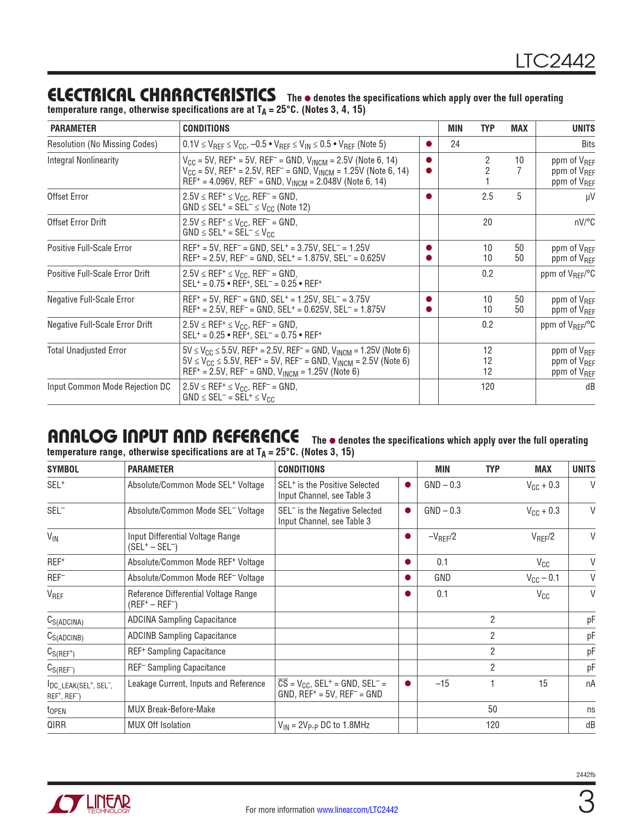
ELECTRICAL CHARACTERISTICS The. denotes the specifications which apply over the full operating
Модельный ряд для этого даташита
Текстовая версия документа
LTC2442
ELECTRICAL CHARACTERISTICS The
l
denotes the specifications which apply over the full operating temperature range, otherwise specifications are at TA = 25°C. (Notes 3, 4, 15) PARAMETER CONDITIONS MIN TYP MAX UNITS
Resolution (No Missing Codes) 0.1V ≤ VREF ≤ VCC, –0.5 • VREF ≤ VIN ≤ 0.5 • VREF (Note 5) l 24 Bits Integral Nonlinearity VCC = 5V, REF+ = 5V, REF– = GND, VINCM = 2.5V (Note 6, 14) l 2 10 ppm of VREF VCC = 5V, REF+ = 2.5V, REF– = GND, VINCM = 1.25V (Note 6, 14) l 2 7 ppm of VREF REF+ = 4.096V, REF– = GND, VINCM = 2.048V (Note 6, 14) 1 ppm of VREF Offset Error 2.5V ≤ REF+ ≤ VCC, REF– = GND, l 2.5 5 µV GND ≤ SEL+ = SEL– ≤ VCC (Note 12) Offset Error Drift 2.5V ≤ REF+ ≤ VCC, REF– = GND, 20 nV/°C GND ≤ SEL+ = SEL– ≤ VCC Positive Full-Scale Error REF+ = 5V, REF– = GND, SEL+ = 3.75V, SEL– = 1.25V l 10 50 ppm of VREF REF+ = 2.5V, REF– = GND, SEL+ = 1.875V, SEL– = 0.625V l 10 50 ppm of VREF Positive Full-Scale Error Drift 2.5V ≤ REF+ ≤ VCC, REF– = GND, 0.2 ppm of VREF/°C SEL+ = 0.75 • REF+, SEL– = 0.25 • REF+ Negative Full-Scale Error REF+ = 5V, REF– = GND, SEL+ = 1.25V, SEL– = 3.75V l 10 50 ppm of VREF REF+ = 2.5V, REF– = GND, SEL+ = 0.625V, SEL– = 1.875V l 10 50 ppm of VREF Negative Full-Scale Error Drift 2.5V ≤ REF+ ≤ VCC, REF– = GND, 0.2 ppm of VREF/°C SEL+ = 0.25 • REF+, SEL– = 0.75 • REF+ Total Unadjusted Error 5V ≤ VCC ≤ 5.5V, REF+ = 2.5V, REF– = GND, VINCM = 1.25V (Note 6) 12 ppm of VREF 5V ≤ VCC ≤ 5.5V, REF+ = 5V, REF– = GND, VINCM = 2.5V (Note 6) 12 ppm of VREF REF+ = 2.5V, REF– = GND, VINCM = 1.25V (Note 6) 12 ppm of VREF Input Common Mode Rejection DC 2.5V ≤ REF+ ≤ VCC, REF– = GND, 120 dB GND ≤ SEL– = SEL+ ≤ VCC
ANALOG INPUT AND REFERENCE The
l
denotes the specifications which apply over the full operating temperature range, otherwise specifications are at TA = 25°C. (Notes 3, 15) SYMBOL PARAMETER CONDITIONS MIN TYP MAX UNITS
SEL+ Absolute/Common Mode SEL+ Voltage SEL+ is the Positive Selected l GND – 0.3 VCC + 0.3 V Input Channel, see Table 3 SEL– Absolute/Common Mode SEL– Voltage SEL– is the Negative Selected l GND – 0.3 VCC + 0.3 V Input Channel, see Table 3 VIN Input Differential Voltage Range l –VREF/2 VREF/2 V (SEL+ – SEL–) REF+ Absolute/Common Mode REF+ Voltage l 0.1 VCC V REF– Absolute/Common Mode REF– Voltage l GND VCC – 0.1 V VREF Reference Differential Voltage Range l 0.1 VCC V (REF+ – REF–) CS(ADCINA) ADCINA Sampling Capacitance 2 pF CS(ADCINB) ADCINB Sampling Capacitance 2 pF CS(REF+) REF+ Sampling Capacitance 2 pF CS(REF–) REF– Sampling Capacitance 2 pF IDC_LEAK(SEL+, SEL–, Leakage Current, Inputs and Reference CS = VCC, SEL+ = GND, SEL– = l –15 1 15 nA REF+, REF–) GND, REF+ = 5V, REF– = GND tOPEN MUX Break-Before-Make 50 ns QIRR MUX Off Isolation VIN = 2VP-P DC to 1.8MHz 120 dB 2442fb For more information www.linear.com/LTC2442 3

 Купить LTC2442IG#TRPBF на РадиоЛоцман.Цены — от 440 до 1 345 ₽


