Datasheet LTC2440 (Analog Devices) - 2
| Производитель | Analog Devices |
| Описание | 24-Bit High Speed Differential ∆∑ ADC with Selectable Speed/Resolution |
| Страниц / Страница | 30 / 2 — ABSOLUTE MAXIMUM RATINGS. PIN CONFIGURATION. (Notes 1,2). ORDER … |
| Формат / Размер файла | PDF / 436 Кб |
| Язык документа | английский |
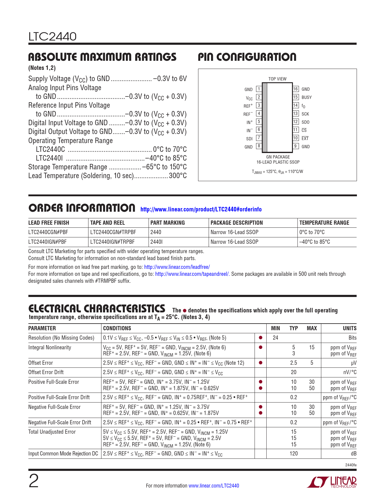
ABSOLUTE MAXIMUM RATINGS. PIN CONFIGURATION. (Notes 1,2). ORDER INFORMATION http://www.linear.com/product/LTC2440#orderinfo

Модельный ряд для этого даташита
Текстовая версия документа
LTC2440
ABSOLUTE MAXIMUM RATINGS PIN CONFIGURATION (Notes 1,2)
Supply Voltage (VCC) to GND ... –0.3V to 6V TOP VIEW Analog Input Pins Voltage GND 1 16 GND to GND ..–0.3V to (VCC + 0.3V) V 2 15 CC BUSY Reference Input Pins Voltage REF+ 3 14 fO to GND ..–0.3V to (VCC + 0.3V) REF– 4 13 SCK Digital Input Voltage to GND ...–0.3V to (VCC + 0.3V) IN+ 5 12 SDO Digital Output Voltage to GND ...–0.3V to (V IN– 6 11 CC + 0.3V) CS Operating Temperature Range 7 SDI 10 EXT LTC2440C ... 0°C to 70°C 8 GND 9 GND LTC2440I ..–40°C to 85°C GN PACKAGE Storage Temperature Range .. –65°C to 150°C 16-LEAD PLASTIC SSOP Lead Temperature (Soldering, 10 sec) ...300°C TJMAX = 125°C, θJA = 110°C/W
ORDER INFORMATION http://www.linear.com/product/LTC2440#orderinfo LEAD FREE FINISH TAPE AND REEL PART MARKING PACKAGE DESCRIPTION TEMPERATURE RANGE
LTC2440CGN#PBF LTC2440CGN#TRPBF 2440 Narrow 16-Lead SSOP 0°C to 70°C LTC2440IGN#PBF LTC2440IGN#TRPBF 2440I Narrow 16-Lead SSOP –40°C to 85°C Consult LTC Marketing for parts specified with wider operating temperature ranges. Consult LTC Marketing for information on non-standard lead based finish parts. For more information on lead free part marking, go to: http://www.linear.com/leadfree/ For more information on tape and reel specifications, go to: http://www.linear.com/tapeandreel/. Some packages are available in 500 unit reels through designated sales channels with #TRMPBF suffix.
ELECTRICAL CHARACTERISTICS The
l
denotes the specifications which apply over the full operating temperature range, otherwise specifications are at TA = 25°C. (Notes 3, 4) PARAMETER CONDITIONS MIN TYP MAX UNITS
Resolution (No Missing Codes) 0.1V ≤ VREF ≤ VCC, –0.5 • VREF ≤ VIN ≤ 0.5 • VREF, (Note 5) l 24 Bits Integral Nonlinearity VCC = 5V, REF+ = 5V, REF– = GND, VINCM = 2.5V, (Note 6) l 5 15 ppm of VREF REF+ = 2.5V, REF– = GND, VINCM = 1.25V, (Note 6) 3 ppm of VREF Offset Error 2.5V ≤ REF+ ≤ VCC, REF– = GND, GND ≤ IN+ = IN– ≤ VCC (Note 12) l 2.5 5 µV Offset Error Drift 2.5V ≤ REF+ ≤ VCC, REF– = GND, GND ≤ IN+ = IN– ≤ VCC 20 nV/°C Positive Full-Scale Error REF+ = 5V, REF– = GND, IN+ = 3.75V, IN– = 1.25V l 10 30 ppm of VREF REF+ = 2.5V, REF– = GND, IN+ = 1.875V, IN– = 0.625V l 10 50 ppm of VREF Positive Full-Scale Error Drift 2.5V ≤ REF+ ≤ VCC, REF– = GND, IN+ = 0.75REF+, IN– = 0.25 • REF+ 0.2 ppm of VREF/°C Negative Full-Scale Error REF+ = 5V, REF– = GND, IN+ = 1.25V, IN– = 3.75V l 10 30 ppm of VREF REF+ = 2.5V, REF– = GND, IN+ = 0.625V, IN– = 1.875V l 10 50 ppm of VREF Negative Full-Scale Error Drift 2.5V ≤ REF+ ≤ VCC, REF– = GND, IN+ = 0.25 • REF+, IN– = 0.75 • REF+ 0.2 ppm of VREF/°C Total Unadjusted Error 5V ≤ VCC ≤ 5.5V, REF+ = 2.5V, REF– = GND, VINCM = 1.25V 15 ppm of VREF 5V ≤ VCC ≤ 5.5V, REF+ = 5V, REF– = GND, VINCM = 2.5V 15 ppm of VREF REF+ = 2.5V, REF– = GND, VINCM = 1.25V, (Note 6) 15 ppm of VREF Input Common Mode Rejection DC 2.5V ≤ REF+ ≤ VCC, REF– = GND, GND ≤ IN– = IN+ ≤ VCC 120 dB 2440fe 2 For more information www.linear.com/LTC2440 Document Outline Features Description Applications Typical Application Absolute Maximum Ratings Pin Configuration Typical Performance Characteristics Pin Functions Typical Application Related Parts

 Купить LTC2440IGN#TRPBF на РадиоЛоцман.Цены — от 565 до 2 642 ₽