Datasheet LTC2439-1 (Analog Devices) - 3
| Производитель | Analog Devices |
| Описание | 8-/16-Channel 16-Bit No Latency ∆Σ™ ADC |
| Страниц / Страница | 30 / 3 — ELECTRICAL CHARACTERISTICS. The. denotes the specifications which apply … |
| Формат / Размер файла | PDF / 583 Кб |
| Язык документа | английский |
ELECTRICAL CHARACTERISTICS. The. denotes the specifications which apply over the full operating

Модельный ряд для этого даташита
Текстовая версия документа
LTC2439-1
ELECTRICAL CHARACTERISTICS The
l
denotes the specifications which apply over the full operating temperature range, otherwise specifications are at TA = 25°C. (Notes 3, 4) PARAMETER CONDITIONS MIN TYP MAX UNITS
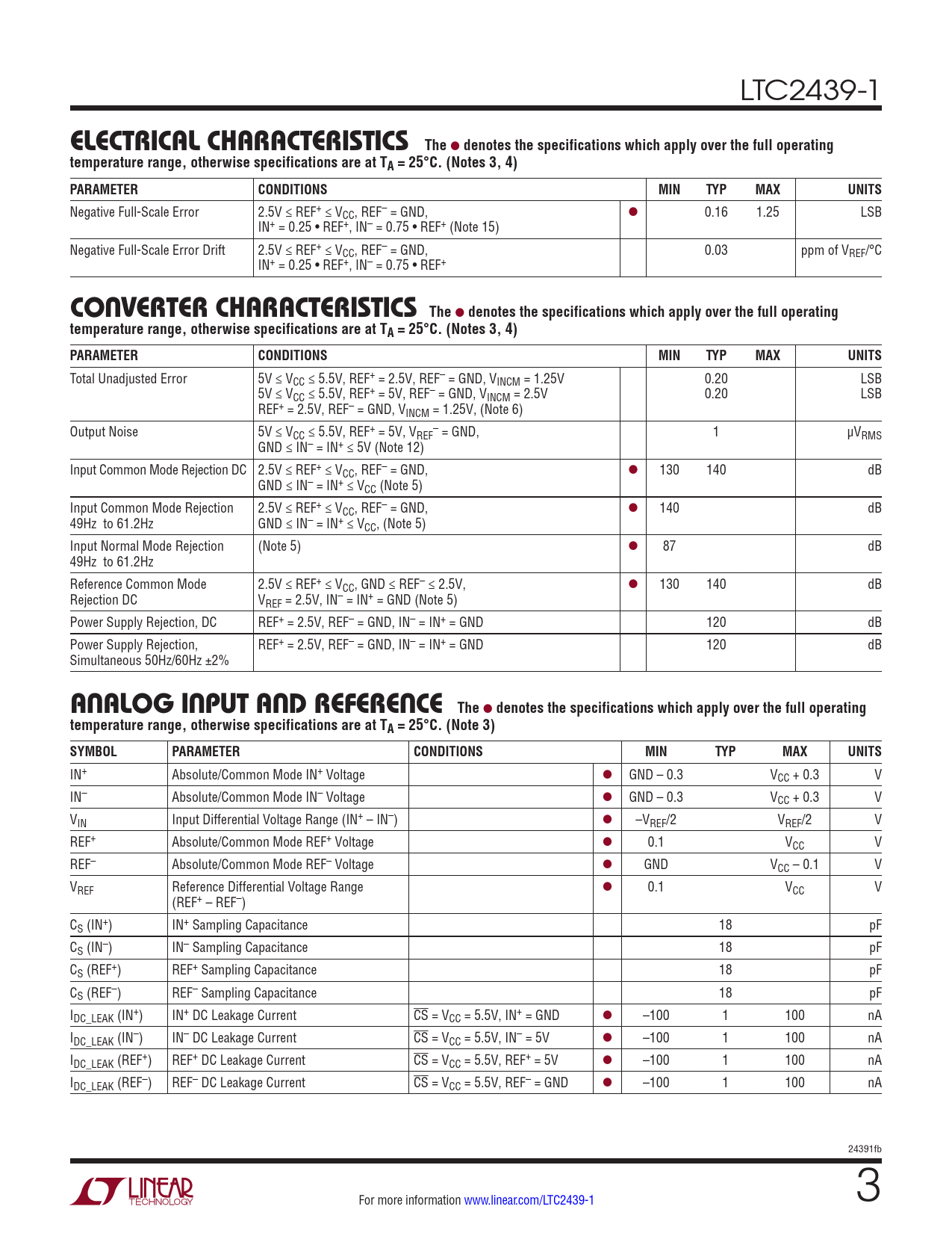
Negative Full-Scale Error 2.5V ≤ REF+ ≤ VCC, REF– = GND, l 0.16 1.25 LSB IN+ = 0.25 • REF+, IN– = 0.75 • REF+ (Note 15) Negative Full-Scale Error Drift 2.5V ≤ REF+ ≤ VCC, REF– = GND, 0.03 ppm of VREF/°C IN+ = 0.25 • REF+, IN– = 0.75 • REF+
CONVERTER CHARACTERISTICS The
l
denotes the specifications which apply over the full operating temperature range, otherwise specifications are at TA = 25°C. (Notes 3, 4) PARAMETER CONDITIONS MIN TYP MAX UNITS
Total Unadjusted Error 5V ≤ VCC ≤ 5.5V, REF+ = 2.5V, REF– = GND, VINCM = 1.25V 0.20 LSB 5V ≤ VCC ≤ 5.5V, REF+ = 5V, REF– = GND, VINCM = 2.5V 0.20 LSB REF+ = 2.5V, REF– = GND, VINCM = 1.25V, (Note 6) Output Noise 5V ≤ V – CC ≤ 5.5V, REF+ = 5V, VREF = GND, 1 µVRMS GND ≤ IN– = IN+ ≤ 5V (Note 12) Input Common Mode Rejection DC 2.5V ≤ REF+ ≤ VCC, REF– = GND, l 130 140 dB GND ≤ IN– = IN+ ≤ VCC (Note 5) Input Common Mode Rejection 2.5V ≤ REF+ ≤ VCC, REF– = GND, l 140 dB 49Hz to 61.2Hz GND ≤ IN– = IN+ ≤ VCC, (Note 5) Input Normal Mode Rejection (Note 5) l 87 dB 49Hz to 61.2Hz Reference Common Mode 2.5V ≤ REF+ ≤ VCC, GND ≤ REF– ≤ 2.5V, l 130 140 dB Rejection DC VREF = 2.5V, IN– = IN+ = GND (Note 5) Power Supply Rejection, DC REF+ = 2.5V, REF– = GND, IN– = IN+ = GND 120 dB Power Supply Rejection, REF+ = 2.5V, REF– = GND, IN– = IN+ = GND 120 dB Simultaneous 50Hz/60Hz ±2%
ANALOG INPUT AND REFERENCE The
l
denotes the specifications which apply over the full operating temperature range, otherwise specifications are at TA = 25°C. (Note 3) SYMBOL PARAMETER CONDITIONS MIN TYP MAX UNITS
IN+ Absolute/Common Mode IN+ Voltage l GND – 0.3 VCC + 0.3 V IN– Absolute/Common Mode IN– Voltage l GND – 0.3 VCC + 0.3 V VIN Input Differential Voltage Range (IN+ – IN–) l –VREF/2 VREF/2 V REF+ Absolute/Common Mode REF+ Voltage l 0.1 VCC V REF– Absolute/Common Mode REF– Voltage l GND VCC – 0.1 V VREF Reference Differential Voltage Range l 0.1 VCC V (REF+ – REF–) CS (IN+) IN+ Sampling Capacitance 18 pF CS (IN–) IN– Sampling Capacitance 18 pF CS (REF+) REF+ Sampling Capacitance 18 pF CS (REF–) REF– Sampling Capacitance 18 pF IDC_LEAK (IN+) IN+ DC Leakage Current CS = VCC = 5.5V, IN+ = GND l –100 1 100 nA IDC_LEAK (IN–) IN– DC Leakage Current CS = VCC = 5.5V, IN– = 5V l –100 1 100 nA IDC_LEAK (REF+) REF+ DC Leakage Current CS = VCC = 5.5V, REF+ = 5V l –100 1 100 nA IDC_LEAK (REF–) REF– DC Leakage Current CS = VCC = 5.5V, REF– = GND l –100 1 100 nA 24391fb For more information www.linear.com/LTC2439-1 3 Document Outline Features Applications Typical Application Absolute Maximum Ratings Order Information Electrical Characteristics Converter Characteristics Analog Input and Reference Digital Inputs and Digital Outputs POWER REQUIREMENTS Timing Characteristics Pin Functions FUNCTIONAL Block Diagram Test CircuitS Applications Information Package Description Revision History Typical Application Related Parts
