Datasheet LTC2175-14, LTC2174-14, LTC2173-14 (Analog Devices) - 4
| Производитель | Analog Devices |
| Описание | 14-Bit, 125Msps Low Power Quad ADCs |
| Страниц / Страница | 34 / 4 — DynaMic accuracy. The. denotes the specifications which apply over the … |
| Формат / Размер файла | PDF / 873 Кб |
| Язык документа | английский |
DynaMic accuracy. The. denotes the specifications which apply over the full operating temperature range,
Модельный ряд для этого даташита
Текстовая версия документа
LTC2175-14/ LTC2174-14/LTC2173-14
DynaMic accuracy The
l
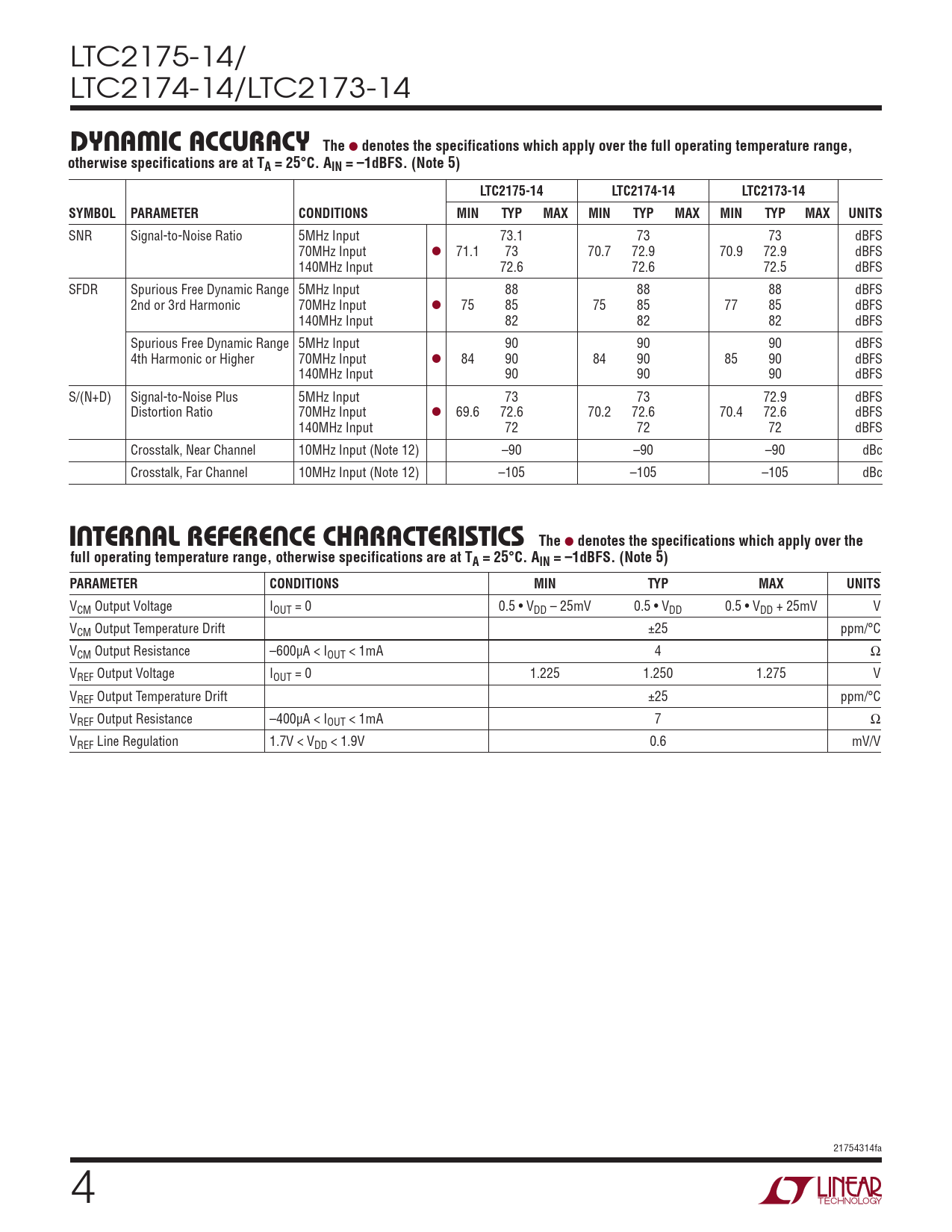
denotes the specifications which apply over the full operating temperature range, otherwise specifications are at TA = 25°C. AIN = –1dBFS. (Note 5) LTC2175-14 LTC2174-14 LTC2173-14 SYMBOL PARAMETER CONDITIONS MIN TYP MAX MIN TYP MAX MIN TYP MAX UNITS
SNR Signal-to-Noise Ratio 5MHz Input 73.1 73 73 dBFS 70MHz Input l 71.1 73 70.7 72.9 70.9 72.9 dBFS 140MHz Input 72.6 72.6 72.5 dBFS SFDR Spurious Free Dynamic Range 5MHz Input 88 88 88 dBFS 2nd or 3rd Harmonic 70MHz Input l 75 85 75 85 77 85 dBFS 140MHz Input 82 82 82 dBFS Spurious Free Dynamic Range 5MHz Input 90 90 90 dBFS 4th Harmonic or Higher 70MHz Input l 84 90 84 90 85 90 dBFS 140MHz Input 90 90 90 dBFS S/(N+D) Signal-to-Noise Plus 5MHz Input 73 73 72.9 dBFS Distortion Ratio 70MHz Input l 69.6 72.6 70.2 72.6 70.4 72.6 dBFS 140MHz Input 72 72 72 dBFS Crosstalk, Near Channel 10MHz Input (Note 12) –90 –90 –90 dBc Crosstalk, Far Channel 10MHz Input (Note 12) –105 –105 –105 dBc
inTernal reFerence characTerisTics The
l
denotes the specifications which apply over the full operating temperature range, otherwise specifications are at TA = 25°C. AIN = –1dBFS. (Note 5) PARAMETER CONDITIONS MIN TYP MAX UNITS
VCM Output Voltage IOUT = 0 0.5 • VDD – 25mV 0.5 • VDD 0.5 • VDD + 25mV V VCM Output Temperature Drift ±25 ppm/°C VCM Output Resistance –600µA < IOUT < 1mA 4 Ω VREF Output Voltage IOUT = 0 1.225 1.250 1.275 V VREF Output Temperature Drift ±25 ppm/°C VREF Output Resistance –400µA < IOUT < 1mA 7 Ω VREF Line Regulation 1.7V < VDD < 1.9V 0.6 mV/V 21754314fa 4 Document Outline Features Applications Description Typical Application Absolute Maximum Ratings Pin Configuration Order Information Converter Characteristics Analog Input Dynamic Accuracy Internal Reference Characteristics Digital Inputs and Outputs Power Requirements Timing Characteristics Timing Diagrams Typical Performance Characteristics Pin Functions Functional Block Diagram Applications Information Typical Applications Package Description Revision History Related Parts

 Купить LTC2174CUKG-14#PBF на РадиоЛоцман.Цены — от 225 до 14 235 ₽


