DatasheetsDatasheet ADA4817-1, ADA4817-2 (Analog …
Datasheet ADA4817-1, ADA4817-2 (Analog Devices)
| Производитель | Analog Devices |
| Описание | Dual, Low Noise, 1 GHz FastFET Op Amplifier |
| Страниц / Страница | 25 / 1 — Low Noise, 1 GHz. FastFET. Op Amps. Data Sheet. ADA4817-1. /ADA4817-2. … |
| Версия | G |
| Формат / Размер файла | PDF / 632 Кб |
| Язык документа | английский |
Low Noise, 1 GHz. FastFET. Op Amps. Data Sheet. ADA4817-1. /ADA4817-2. FEATURES. CONNECTION DIAGRAMS. High speed. TOP VIEW

Текстовая версия документа
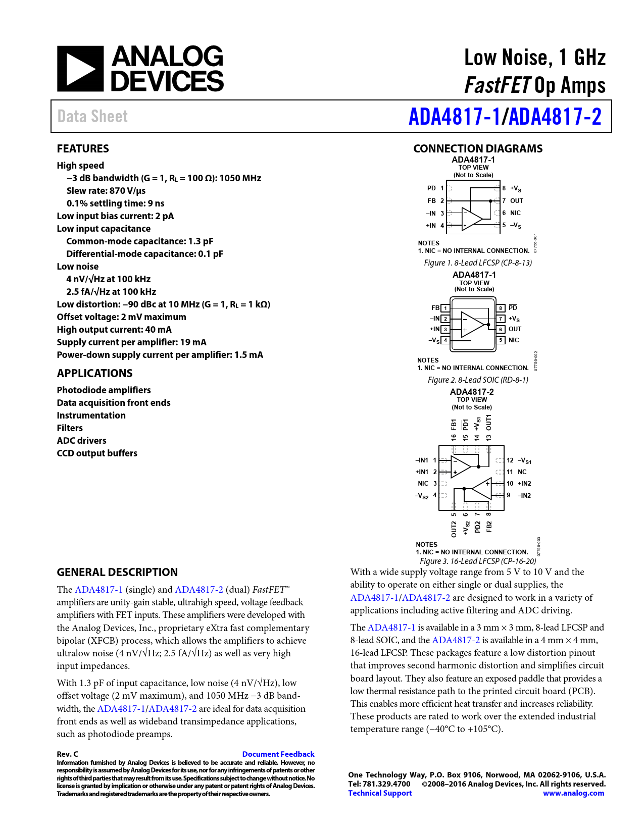
Low Noise, 1 GHz FastFET Op Amps Data Sheet ADA4817-1 /ADA4817-2 FEATURES CONNECTION DIAGRAMS ADA4817-1 High speed TOP VIEW −3 dB bandwidth (G = 1, R (Not to Scale) L = 100 Ω): 1050 MHz Slew rate: 870 V/μs PD 1 8 +VS 0.1% settling time: 9 ns FB 2 7 OUT Low input bias current: 2 pA –IN 3 6 NIC 5 –V Low input capacitance +IN 4 S Common-mode capacitance: 1.3 pF
001 6-
NOTES Differential-mode capacitance: 0.1 pF 1. NIC = NO INTERNAL CONNECTION.
0775
Low noise
Figure 1. 8-Lead LFCSP (CP-8-13)
ADA4817-1 4 nV/√Hz at 100 kHz TOP VIEW 2.5 fA/√Hz at 100 kHz (Not to Scale) Low distortion: −90 dBc at 10 MHz (G = 1, RL = 1 kΩ) FB 1 8 PD Offset voltage: 2 mV maximum –IN 2 7 +VS High output current: 40 mA +IN 3 6 OUT Supply current per amplifier: 19 mA –VS 4 5 NIC Power-down supply current per amplifier: 1.5 mA
2
NOTES
00 56-
1. NIC = NO INTERNAL CONNECTION. APPLICATIONS
077 Figure 2. 8-Lead SOIC (RD-8-1)
Photodiode amplifiers ADA4817-2 Data acquisition front ends TOP VIEW (Not to Scale) Instrumentation 1 T1 S1 Filters FB PD1 +V OU 6 5 4 3 ADC drivers 1 1 1 1 CCD output buffers –IN1 1 12 –VS1 +IN1 2 11 NC NIC 3 10 +IN2 –V 4 9 S2 –IN2 5 6 7 8 2 T2 S2 PD2 FB OU +V
-003
NOTES 1. NIC = NO INTERNAL CONNECTION.
07756 Figure 3. 16-Lead LFCSP (CP-16-20)
GENERAL DESCRIPTION
With a wide supply voltage range from 5 V to 10 V and the The ADA4817-1 (single) and ADA4817-2 (dual) FastFET™ ability to operate on either single or dual supplies, the amplifiers are unity-gain stable, ultrahigh speed, voltage feedback ADA4817-1/ADA4817-2 are designed to work in a variety of amplifiers with FET inputs. These amplifiers were developed with applications including active filtering and ADC driving. the Analog Devices, Inc., proprietary eXtra fast complementary The ADA4817-1 is available in a 3 mm × 3 mm, 8-lead LFCSP and bipolar (XFCB) process, which allows the amplifiers to achieve 8-lead SOIC, and the ADA4817-2 is available in a 4 mm × 4 mm, ultralow noise (4 nV/√Hz; 2.5 fA/√Hz) as well as very high 16-lead LFCSP. These packages feature a low distortion pinout input impedances. that improves second harmonic distortion and simplifies circuit With 1.3 pF of input capacitance, low noise (4 nV/√Hz), low board layout. They also feature an exposed paddle that provides a offset voltage (2 mV maximum), and 1050 MHz −3 dB band- low thermal resistance path to the printed circuit board (PCB). width, the ADA4817-1/ADA4817-2 are ideal for data acquisition This enables more efficient heat transfer and increases reliability. front ends as well as wideband transimpedance applications, These products are rated to work over the extended industrial such as photodiode preamps. temperature range (−40°C to +105°C).
Rev. C Document Feedback Information furnished by Analog Devices is believed to be accurate and reliable. However, no responsibility is assumed by Analog Devices for its use, nor for any infringements of patents or other rights of third parties that may result from its use. Specifications subject to change without notice. No One Technology Way, P.O. Box 9106, Norwood, MA 02062-9106, U.S.A. license is granted by implication or otherwise under any patent or patent rights of Analog Devices. Tel: 781.329.4700 ©2008–2016 Analog Devices, Inc. All rights reserved. Trademarks and registered trademarks are the property of their respective owners. Technical Support www.analog.com
Document Outline FEATURES APPLICATIONS CONNECTION DIAGRAMS GENERAL DESCRIPTION TABLE OF CONTENTS REVISION HISTORY SPECIFICATIONS ±5 V OPERATION 5 V OPERATION ABSOLUTE MAXIMUM RATINGS THERMAL RESISTANCE MAXIMUM SAFE POWER DISSIPATION ESD CAUTION PIN CONFIGURATIONS AND FUNCTION DESCRIPTIONS TYPICAL PERFORMANCE CHARACTERISTICS TEST CIRCUITS THEORY OF OPERATION CLOSED-LOOP FREQUENCY RESPONSE NONINVERTING CLOSED-LOOP FREQUENCY RESPONSE INVERTING CLOSED-LOOP FREQUENCY RESPONSE WIDEBAND OPERATION DRIVING CAPACITIVE LOADS THERMAL CONSIDERATIONS POWER-DOWN OPERATION CAPACITIVE FEEDBACK HIGHER FREQUENCY ATTENUATION LAYOUT, GROUNDING, AND BYPASSING CONSIDERATIONS SIGNAL ROUTING POWER SUPPLY BYPASSING GROUNDING EXPOSED PADDLE LEAKAGE CURRENTS INPUT CAPACITANCE INPUT-TO-INPUT/OUTPUT COUPLING APPLICATIONS INFORMATION LOW DISTORTION PINOUT WIDEBAND PHOTODIODE PREAMP HIGH SPEED JFET INPUT INSTRUMENTATION AMPLIFIER ACTIVE LOW-PASS FILTER (LPF) OUTLINE DIMENSIONS ORDERING GUIDE